ADM-PA101 User Manual
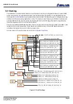
quad. This programable clock has a default 156.25MHz reference clock. This clock frequency can be changed to
any arbitrary clock frequency up to 350MHz by re-programing the Si5338 reprogrammable clock oscillator. See
details on avr2util in the section:
.
See net names MGT_PROGCLK_*_PIN_P/N in the
3.2.6 FMC Clocks
The FMC specification defines 6 gigabit transceiver clocks (GBTCLK*), one for each four high speed serial lanes.
By default only GBTCLK2, GBTCLK3, and GBTCLK6 are connected. The other three can be connected through
a build option custimzation.
The specification also defines 4 general clocks (CLK*_M2C and CLK*_BDIR). Each of these clocks have
external AC coupling, DC bias, and 100 ohm termination (suitable for LVDS).
See ANSI/VITA 46.0 and ANSI/VITA 57.4 for full details of the FMC specification.
See net names GBTCLK*_PIN_P/N, CLK*_M2C_PIN_P/N, and CLK*_BIDIR_PIN_P/N in the
The ACAP quads connected to the FMC site are also configured such that they can be clocked from the Si5328
jitter attenuator, or the onboard Si5338 clock synthesizer.
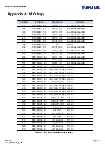
Pin locations of net names SI5328_*_OUT_P/N and MGT_PROGCLK_*_P/N can be located in the
3.2.7 Samtec FireFly Clock
The FireFly clock has a default 350MHz reference clock. This clock frequency can be changed to any arbitrary
clock frequency up to 350MHz by re-programing the Si5338 reprogrammable clock oscillator. See details on
.
See net names FIREFLY_CLK_PIN_P/N in the
for pin locations.
3.2.8 Memory Clocks
Each of the two memory banks has their own buffered 300MHz reference clock. This clock frequency can be
changed to any arbitrary clock frequency up to 350MHz by re-programing the Si5338 reprogrammable clock
oscillator. See details on avr2util in the section:
.
See net names MEM_CLK_*_PIN_P/N in the
See
for mor information on the memory banks and their physical locations.
These clocks are not fabric accessible, but are reserved for the Versal DDR4 cores.
Page 11
Functional Description
ad-ug-1430_v1_2.pdf


