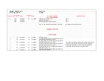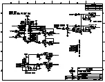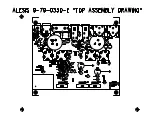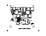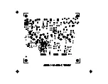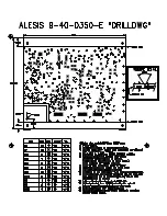
UB0MNF - Main PCB Rev F
Last Revised:
RevChange Document
3/17/2006
SCH PCB CAM
Suggested
by:
DATE
Performed
by:
DATE
Description of change:
Reason for change:
TOP LEVEL CHANGES
x
x
SOP
3/13/2006
JK
3/17/2006
Change all text from Rev E to F
SOP
SOP
3/13/2006
update all Part Types
SOP
SOP
3/13/2006
Review/Integrate all outstanding ECNs
SOP
Note: ***A new solderpaste stencil IS NOT required***
No SMD components were moved.
SCHEMATIC CHANGES
PCB CHANGES
x
JK
3/14/2006
JK
3/17/2006
Flood power plane.
x
YH
3/16/2006
JK
3/16/2006
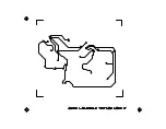
The bottom layer pads of C75's negative terminal and
C76's positive terminal are too close.
x
YH
3/16/2006
JK
3/16/2006
The bottom layer pads of C43's negative terminal and
C44's positive terminal are too close.
x
YH
3/16/2006
JK
3/16/2006
The bottom layer pads of C57's negative terminal and
C68's positive terminal are too close.
x
YH
3/16/2006
JK
3/16/2006
The bottom layer pad of C40's negative terminal is too
close to C41's +3.3V via.
x
YH
3/16/2006
JK
3/16/2006
The bottom layer pad of C60's negative terminal is too
close to one of R68's pads.
The leads of the thru-hole components at these locations, after
being bent during the auto-insertion process (to prevent the
components from falling out), tend to short out against the
neighboring pads during the wave-solder process.
Summary of Contents for IO|2
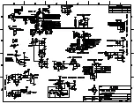
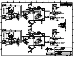
Page 5: ...ALESIS IO 2 UB0 SCHEMATIC AND PCB FILES Confidential Alesis Service Manual 8 31 0137 A ...
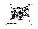
Page 6: ...MAIN PCB REV F Confidential Alesis Service Manual 8 31 0137 A ...
Page 7: ......
Page 8: ......
Page 9: ......
Page 10: ......
Page 11: ......
Page 12: ......
Page 13: ......
Page 14: ......
Page 15: ......
Page 16: ......
Page 17: ......
Page 18: ......
Page 19: ......
Page 20: ......
Page 21: ......
Page 22: ......
Page 24: ...MAIN PCB REV E Confidential Alesis Service Manual 8 31 0137 A ...
Page 25: ......
Page 26: ......
Page 27: ......
Page 28: ......
Page 29: ......
Page 30: ......
Page 31: ......
Page 32: ......
Page 33: ......
Page 34: ......
Page 35: ......
Page 36: ......
Page 37: ......
Page 38: ......
Page 39: ......
Page 40: ......
Page 42: ...MAIN PCB REV D Confidential Alesis Service Manual 8 31 0137 A ...
Page 43: ......
Page 44: ......
Page 45: ......
Page 46: ......
Page 47: ......
Page 48: ......
Page 49: ......
Page 50: ......
Page 51: ......
Page 52: ......
Page 53: ......
Page 54: ......
Page 55: ......
Page 56: ......
Page 57: ......
Page 58: ......
Page 60: ...MAIN PCB REV C Confidential Alesis Service Manual 8 31 0137 A ...
Page 61: ......
Page 62: ......
Page 63: ......
Page 64: ......
Page 65: ......
Page 66: ......
Page 67: ......
Page 68: ......
Page 69: ......
Page 70: ......
Page 71: ......
Page 72: ......
Page 73: ......
Page 74: ......
Page 75: ......
Page 76: ......
Page 79: ...Solder a 100ohm resistor onto PCB to bridge the cut 4 places ...
Page 80: ...FRONT PANEL PCB REV C Confidential Alesis Service Manual 8 31 0137 A ...
Page 81: ......
Page 82: ......
Page 83: ......
Page 84: ......
Page 85: ......
Page 86: ......
Page 87: ......
Page 88: ......
Page 89: ......
Page 91: ...FRONT PANEL PCB REV B Confidential Alesis Service Manual 8 31 0137 A ...
Page 92: ......
Page 93: ......
Page 94: ......
Page 95: ......
Page 96: ......
Page 97: ......
Page 98: ......
Page 99: ......
Page 100: ......
Page 102: ...ALESIS IO 2 UB0 ECN HISTORY Confidential Alesis Service Manual 8 31 0137 A ...
Page 103: ......
Page 105: ...ALESIS IO 2 UB0 BOM Confidential Alesis Service Manual 8 31 0137 A ...


