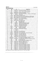

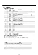

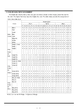


condition at Ta = 25
±
2
℃
and I
L
= 4.0 ~ 5.0 mA
RMS
.
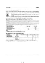
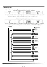
Note (5) The power supply capacity should be higher than the total inverter power consumption P
BL
. Since
the pulse width modulation (PWM) mode was applied for backlight dimming, the driving current
changed as PWM duty on and off. The transient response of power supply should be considered
for the changing loading when inverter dimming.
Note (6) To enhance the performance of backlight, the power consumption will increase to 1.5 times of the
typical power consumption P
BL
in the power on stage and 20 seconds later it will return to typical
value. Thus, the power source capacity for inverter should be considered to supply the initial
power consumption at power on duration.
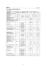
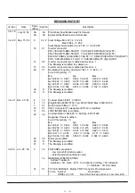
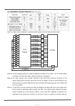
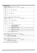
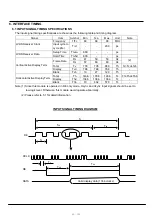
3.2.3 INVERTER INTERFACE CHARACTERISTICS
Value
Parameter Symbol
Test
Condition
Min.
Typ.
Max.
Unit Note
ON
-
2.0
-
5.0
V
On/Off Control
Voltage
OFF
V
BLON
-
0
-
0.8
V
HI
-
2.0
-
5.0
V
Internal/External
PWM Select Voltage LO
V
SEL
-
0
-
0.8
V
MAX
-
-
3.0
V minimum
duty ratio
Internal PWM
Control Voltage
MIN
V
IPWM
V
SEL
= L
-
0
-
V maximum
duty ratio
HI
2.0
-
5.0
V duty on
External PWM
Control Voltage
LO
V
EPWM
V
SEL
= H
0
-
0.8
V duty fff
Control Signal Rising Time
T
r
-
-
-
100
ms
Control Signal Falling Time
T
f
-
-
-
100
ms
PWM Signal Rising Time
T
PWMR
-
-
-
50
us
PWM Signal Falling Time
T
PWMF
-
-
-
50
us
Input impedance R
IN
-
1
-
-
M
Ω
BLON Delay Time
T
on
-
500
-
-
ms
BLON Off Time
T
off
-
500
-
-
ms
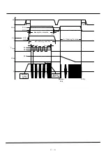
Note (1) The SEL signal should be valid before backlight turns on by BLON signal. It is inhibited to change
the internal/external PWM selection (SEL) during backlight turn on period.
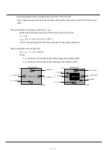
Note (2) The power sequence and control signal timing are shown as the following figure.
86/129
Summary of Contents for LCT3285TAJ
Page 1: ......
Page 5: ... 3 129 ...
Page 6: ... 0 12 0 12 0 0 1 3 124 1 3 5 3 6 27 8 6 27 1 7 12 60 26 9 1 7 12 2 1 7 12 3 1 4 2 4 129 ...
Page 7: ...12 6 6 7 1 3 0 1 3 1 3 7 3 4 4 5 129 ...
Page 40: ...38 129 ...
Page 41: ...39 129 ...
Page 42: ...40 129 ...
Page 43: ...41 129 ...
Page 44: ...42 129 ...
Page 45: ...43 129 ...
Page 46: ...44 129 ...
Page 47: ...45 129 ...
Page 48: ...46 129 ...
Page 49: ...47 129 ...
Page 50: ...48 129 ...
Page 51: ...49 129 ...
Page 52: ...50 129 ...
Page 53: ...51 129 ...
Page 54: ...52 129 ...
Page 55: ...53 129 ...
Page 56: ...54 129 ...
Page 57: ...55 129 ...
Page 58: ...56 129 ...
Page 59: ...57 129 ...
Page 60: ...58 129 ...
Page 61: ...59 129 ...
Page 62: ...60 129 ...
Page 63: ...61 129 ...
Page 64: ...62 129 ...
Page 72: ...70 129 ...
Page 73: ...71 129 ...
Page 74: ...72 129 ...
Page 75: ...73 129 ...
Page 76: ...74 129 ...
Page 77: ...75 129 ...
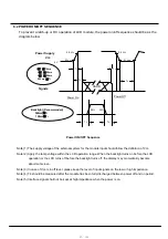
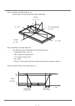
Page 106: ...Figure 9 2 Packing method 104 129 ...
Page 108: ...11 MECHANICAL CHARACTERISTICS 奇美電子股份有限公司 CHI MEI 106 129 ...
Page 109: ...奇美電子股份有限公司 CHI MEI 107 129 ...
Page 110: ...108 129 ...
Page 120: ...118 129 ...
Page 121: ...119 129 ...
Page 122: ...120 129 ...
Page 128: ...3 Cables Standard for Upgrade Board 126 129 ...
Page 129: ...127 129 ...
Page 130: ...128 129 ...
Page 131: ...129 129 ...