-39-
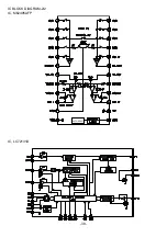
IC DESCRIPTION-1/3 (LA9241ML)-1/2
1
2
3
4
5
6
7
8
9
10
11
12
13
14
15
16
17
18
19
20
21
22
23
24
25
26
27
28
29
30, 31
32, 33
34
35
FIN2
FIN1
E
F
TB
TE–
TE
TESI
SCI
TH
TA
TD–
TD
JP
TO
FD
FD–
FA
FA–
FE
FE–
AGND
SP
SP–
SPG
SP–
SPD
SLEQ
SLD
SL–, SL+
JP–, JP+
TGL
TOFF
I
I
I
I
I
I
O
I
I
I
O
I
I
I
O
O
I
I
I
O
I
—
—
O
I
I
O
I
O
I
I
I
I
Pin to which external pickup photo diode is connected. RF signal is created by adding with the
FIN1 pin signal. FE signal is created by subtracting from the FIN1 pin signal.
Pin to which external pickup photo diode is connected.
Pin to which external pickup photo diode is connected. TE signal is created by subtracting from
the F pin signal.
Pin to which external pickup photo diode is connected.
DC component of the TE signal is input.
Pin to which external resistor setting the TE signal gain is connected between the TE pin.
TE signal output pin.
TES “Track Error Sense” comparator input pin. TE signal is passed through a band-pass filter
then input.
Shock detection signal input pin.
Tracking gain time constant setting pin.
TA amplifier output pin.
Pin to which external tracking phase compensation constants are connected between the TD and
VR pins.
Tracking phase compensation setting pin.
Tracking jump signal (kick pulse) amplitude setting pin.
Tracking control signal output pin.
Focusing control signal output pin.
Pin to which external focusing phase compensation constants are connected between the FD and
FA pins.
Pin to which external focusing phase compensation constants are connected between the FD–
and FA– pins.
Pin to which external focusing phase compensation constants are connected between the FA and
FE pins.
FE signal output pin.
Pin to which external FE signal gain setting resistor is connected between the FE pin.
Analog signal GND.
Single ended output of the CV+ and CV– pin input signal.
Spindle amp input.
Pin to which external spindle gain setting resistor in 12 cm mode is connected.
Pin to which external spindle phase compensation constants are connected together with SPD
pin.
Spindle control signal output pin.
Pin to which external sled phase compensation constants are connected.
Sled control signal output pin.
Sled advance signal input pin from microprocessor.
Tracking jump signal input pin from DSP.
Tracking gain control signal input from DSP. Low gain when TGL = H.
Tracking off control signal input pin from DSP. Off when TOFF = H.
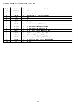
Pin No.
Pin Name
I/O
Description
Summary of Contents for XR-M161HS(S)
Page 23: ... 22 FL ZCL 8 GRID ASSIGNMENT ANODE CONNECTION 1 1 GRID ASSIGNMENT ANODE CONNECTION ...
Page 39: ... 38 IC M62495AFP AUTO RESET IC BLOCK DIAGRAM 2 2 IC LC72131D ...
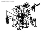
Page 51: ... 50 CD MECHANISM EXPLODED VIEW 1 2 DA 11T3C A M2 PIN 3 SW1 MOTOR C B 4 3 2 1 ...
Page 53: ... 52 CD MECHANISM EXPLODED VIEW 2 2 KSM 213CDM 1 2 COVER 3 4 5 SPINDLE MOTOR M3 MOTOR C B A M2 ...

