


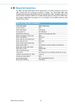
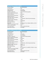
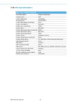


79
MIC-3399 User Manual
Ap
pe
nd
ix A
Pin
A
ss
ign
m
en
ts
A.6
On-Board Connector
Table A.6: SATA1 Daughter Board Connector
1
GND
2
GND
3
S
4
S
5
SATA0_TX-
6
SATA1_TX-
7
GND
8
GND
9
SATA0_RX-
10
SATA1_RX-
11
S
12
S
13
GND
14
GND
15
GND
16
GND
17
VCC5
18
VCC3
19
VCC5
20
VCC3
Table A.7: XMC1 Connector
Pin A
B
C
D
E
F
1
PERX_P0
PERX_N0
+3.3V
PERX_P1
PERX_N1
VPWR(+5V)
2
GND
GND
NC
GND
GND
PRST#
3
PERX_P2
PERX_N2
+3.3V
PERX_P3
PERX_N3
VPWR(+5V)
4
GND
GND
NC
GND
GND
NC
5
PERX_P4
PERX_N4
+3.3V
PERX_P5
PERX_N5
VPWR(+5V)
6
GND
GND
NC
GND
GND
+12V
7
PERX_P6
PERX_N6
+3.3V
PERX_P7
PERX_N7
VPWR(+5V)
8
GND
GND
NC
GND
GND
-12V
9
NC
NC
NC
NC
NC
VPWR(+5V)
10 GND
GND
NC
GND
GND
GA0
11 PETX_P0
PETX_N0
NC
PETX_P1
PETX_N1
VPWR(+5V)
12 GND
GND
GA1
GND
GND
MPRE
-
SENT#
13 PETX_P2
PETX_N2
NC
PETX_P3
PETX_N3
VPWR(+5V)
14 GND
GND
GA2
GND
GND
TBD_SDA
15 PETX_P4
PETX_N4
NC
PETX_P5
PETX_N5
VPWR(+5V)
16 GND
GND
NC
GND
GND
TBD_SCL
17 PETX_P6
PETX_N6
NC
PETX_P7
PETX_N7
NC
18 GND
GND
FPGAIO1 GND
GND
NC
19 CLK CLK_100MHz- FPGAIO2 NC(WAKE#) NC
NC
Summary of Contents for MIC-3399
Page 8: ...MIC 3399 User Manual viii...
Page 29: ...Chapter 2 2 AMI BIOS Setup This chapter describes how to configure the AMI BIOS...
Page 47: ...35 MIC 3399 User Manual Chapter 2 AMI BIOS Setup 2 3 3 8 Southbridge Figure 2 19 Southbridge...
Page 63: ...Chapter 3 3 IPMI Configuration This chapter describes IPMI con figuration for MIC 3399...
Page 85: ...Appendix A A Pin Assignments This appendix provides the pin assignments...
Page 94: ...MIC 3399 User Manual 82...
Page 97: ...Appendix C C FPGA Specifications This appendix describes FPGA configuration...
Page 99: ...87 MIC 3399 User Manual Appendix C FPGA Specifications...