background image

BIOS Setup

 79

cPCI-3610

8.3.7

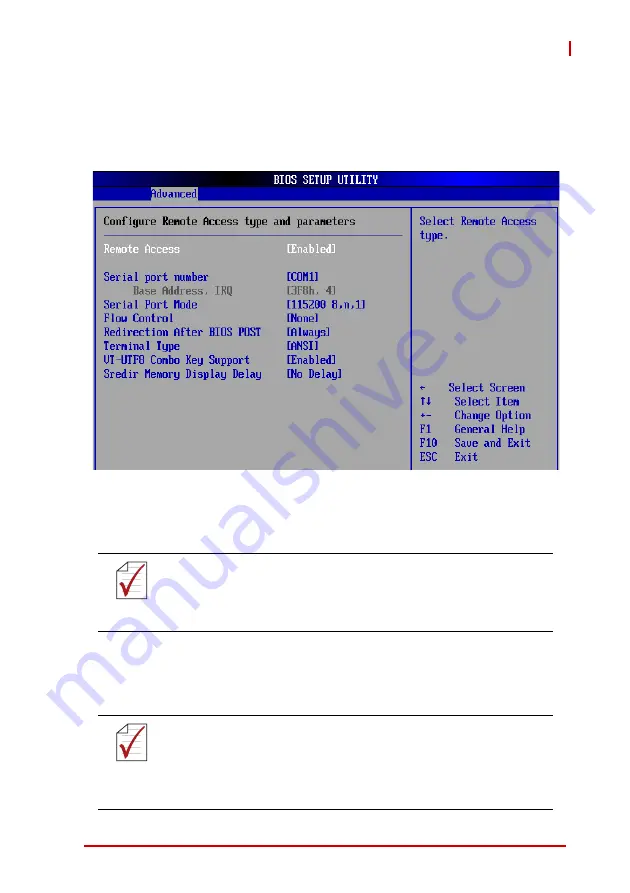
Remote Access Configuration

Remote access configuration provides the settings to allow remote
access by another computer to get POST messages and send
commands through serial port access. 

Remote Access

Select this option to Enable or Disable the BIOS remote access
feature.

Serial Port Number

Select the serial port you want to use for the remote access
interface. Options: COM1, COM2, COM3.

NOTE:

NOTE:

Enabling Remote Access requires a dedicated serial port con-
nection. When the assigned serial port is disabled, Remote 
Access should also be disabled to prevent the system from 
booting abnormally.

NOTE:

NOTE:

If you have changed the resource assignment of the serial 
ports in Advanced> SuperIO Configuration, you must Save 
Changes and Exit, reboot the system, and enter the setup 
menu again in order to see those changes reflected in the 
available Remote Access options.

Summary of Contents for cPCI-3610 Series

Page 1: ...Advance Technologies Automate the World Manual Rev 2 00 Revision Date June 2 2010 Part No 50 15070 1000 cPCI 3610 Series 3U CompactPCI Dual Core Intel Atom Processor Blade User s Manual ...

Page 2: ...Revision History Revision Release Date Description of Change s 2 00 2010 06 02 Initial Release ...

Page 3: ...ven if advised of the possibility of such damages Environmental Responsibility ADLINK is committed to fulfill its social responsibility to global environmental preservation through compliance with the Euro pean Union s Restriction of Hazardous Substances RoHS direc tive and Waste Electrical and Electronic Equipment WEEE directive Environmental protection is a top priority for ADLINK We have enforc...

Page 4: ...ription Describes the cPCI 3610 main functions Chapter 4 Board Interfaces Describes the cPCI 3610 board interfaces Chapter 5 Getting Started Describes the installation of compo nents to the cPCI 3610 and rear transition modules Chapter 6 Driver Installation Provides information on how to install the cPCI 3610 device drivers Chapter 7 Utilities Describes the utilities of the cPCI 3610 Series Chapte...

Page 5: ...erly NOTE NOTE Additional information aids and tips that help users perform tasks CAUTION Information to prevent minor physical injury component dam age data loss and or program corruption when trying to com plete a task WARNING Information to prevent serious physical injury component damage data loss and or program corruption when trying to complete a specific task ...

Page 6: ...vi Preface This page intentionally left blank ...

Page 7: ... 5 Package Contents 5 2 Specifications 7 2 1 cPCI 3610 Specifications 7 2 2 I O Connectivity Table 9 2 3 Power Requirements 10 3 Functional Description 13 3 1 Processor 13 3 2 Chipset 16 3 3 Super I O 16 3 4 Battery 17 3 5 PMC XMC 17 4 Board Interfaces 19 4 1 cPCI 3610 Blade Board Layout 19 4 2 cPCI 3610 Blade Assembly Layout 20 4 3 cPCI 3610D Blade Assembly Layout 21 4 4 cPCI 3610P Blade Assembly...

Page 8: ...the Chassis 54 5 5 RTM Installation cPCI R3610 T 55 6 Driver Installation 57 7 Utilities 59 7 1 Watchdog Timer 59 7 2 Preboot Execution Environment PXE 64 8 BIOS Setup 65 8 1 Starting the BIOS 65 8 2 Main Setup 69 8 3 Advanced BIOS Setup 70 8 3 1 CPU Configuration 71 8 3 2 IDE Configuration 73 8 3 3 Super IO Configuration 74 8 3 4 Hardware Health Configuration 75 8 3 5 USB Configuration 76 8 3 6 A...

Page 9: ...Table of Contents ix cPCI 3610 8 6 Security Setup 84 8 7 Chipset Setup 87 8 8 Exit Menu 88 Important Safety Instructions 91 Getting Service 93 ...

Page 10: ...x Table of Contents This page intentionally left blank ...

Page 11: ...igure 4 1 cPCI 3610 Blade Board Layout 19 Figure 4 2 cPCI 3610 Assembly Layout 20 Figure 4 3 cPCI 3610D Board Layout 21 Figure 4 4 cPCI 3610 cPCI 3610D Front Panel Layout 23 Figure 4 5 cPCI 3610P Front Panel Layout 24 Figure 4 6 cPCI R3610T RTM Board Layout 25 Figure 4 7 cPCI R3610 T RTM Front Panel 26 ...

Page 12: ...xii List of Figures This page intentionally left blank ...

Page 13: ...l ATA Connector on DB 3610L2 Pin Definition 31 Table 4 11 CompactFlash Connector Pin Definition 32 Table 4 12 DB 3610CF Connector Pin Definition 33 Table 4 13 DB 3610L2 Connector Pin Definition 34 Table 4 14 DB 3UMC Connector Pin Definition 35 Table 4 15 PMC Connector Pin Definitions 36 Table 4 16 XMC Connector Pin Definition 38 Table 4 17 CompactPCI J1 Connector Pin Definition 39 Table 4 18 Compa...

Page 14: ...xiv List of Tables This page intentionally left blank ...

Page 15: ...memory up to 2GB integrated graphics on the CPU IDE CompactFlash slot and 2 5 SATA HDD cPCI 3610D P and one PMC XMC site cPCI 3610P Front panel I O includes 2x USB 2x GbE VGA and additional 2x USB COM KB MS and line in out for the 8 12 HP cPCI 3610D P models The optional Rear Transition Module RTM provides 2x SATA 2x GbE 1x USB 2x COM and VGA ports One PCI Express x1 port GPIO and SMBus signals ar...

Page 16: ...e channel DDR2 667 800 SDRAM soldered onboard up to 2GB X 32bit 33MHz CompactPCI Interface based on PCI specifica tions X Optional 32bit 66MHz PMC or PCI Express x1 XMC site X VGA port on front or switchable to RTM X Two PCI Express Gigabit Ethernet egress ports configurable to RTM by software X One IDE CompactFlash socket X Line in and Line out ports on front panel X 2 5 SATA HDD onboard on 8HP 1...

Page 17: ...I COM1 KB MS PCIe x1 GbE 1 SATA 1 1x USB USB 3 4 Intel Atom Processor N450 D410 D510 Line in Line out J1 Intel 82574L PCIe x1 GbE 2 GbE 1 2 2 5 HDD Codec PMC XMC PCIe x1 PCIe x1 32b 66M PCI IT8783F LPC Intel 82574L COM2 COM3 SATA 2 3 PCI 32b 33M PCIe x1 GPIO SMBus CF IDE BIOS SPI Soldered Up to 2GB DDR2 667 Intel ICH8M RGB COM2 3 HD Pericom PI7C9X110 ...

Page 18: ...3610L2 riser card onboard provides 2x USB COM PS 2 KB MS Line in Line out ports X cPCI 3610P 12HP width triple slot 3U CompactPCI fea turing Atom N450 D410 or D510 processor 1GB or 2GB memory soldered onboard CompactFlash slot 2x USB 2x GbE VGA The DB 3610L2 riser card onboard on the 2nd layer provides 2x USB COM PS 2 KB MS Line in Line out ports The DB 3UMC riser card on the 3rd layer provides on...

Page 19: ...PS 2 combo port 8HP 12HP version only X 2 5 HDD accessory pack 8HP 12HP version only X ADLINK All in One CD X User s manual Rear Transition Module X cPCI R3610 8HP width 50mm depth Rear Transition Mod ule with 2x COM USB 2x GbE 2x SATA VGA X cPCI R3610T 8HP width 80mm depth Rear Transition Module with 2x COM USB 2x GbE 2x SATA VGA NOTE NOTE The contents of non standard cPCI 3610 configurations may...

Page 20: ...6 Introduction This page intentionally left blank ...

Page 21: ...capacity dependent on memory process technology DDR2 667 for N450 processor DDR2 800 for D410 D510 processors BIOS AMIBIOS8 16Mbit SPI flash memory CompactPCI Bus PCI 32bit 33MHz 3 3V 5V universal V I O Supports operation in system slot only Gigabit Ethernet Two PCI Express x1 Intel 82574L GbE controllers Two egress 10 100 1000BASE T ports configurable to J2 RTM by software setting Graphics Integr...

Page 22: ...000BASE T Ethernet ports Analog DB 15 VGA port 8HP cPCI 3610D 4x USB 2 0 ports 2x 10 100 1000BASE T Ethernet ports Analog DB 15 VGA port DB 9 RS 232 422 485 485 port PS 2 Keyboard Mouse combo port Line in and Line out ports cPCI R3610 T 2x USB 2 0 ports 10 100 1000BASE T Ethernet port 2x DB 9 RS 232 serial ports OS Compatibility Microsoft Windows XP Professional x64 Edition Microsoft Windows Vista...

Page 23: ...HP cPCI 3610P 12HP cPCI R3610 T Front I O Onboard Front I O Onboard Front I O Onboard Front I O Onboard Gigabit Ethernet Y x2 Y x2 Y x2 Y x2 1 COM Y Y Y x2 USB 2 0 Y x2 Y x4 Y x4 Y VGA Y Y Y Y 1 Serial ATA Y 2 5 HD Y 2 5 HD Y x2 7 pin CF Y Y Y PS 2 KB MS Y Y Line in Y Y Line out Y Y PMC XMC Y GP LED Y x2 Y x2 Y x2 Reset Btn Y Y Y ...

Page 24: ... able to provide at least three times as much power as the entire system requires of each voltage The tolerance of the voltage lines described in the CompactPCI specification PICMG 2 0 R3 0 is 5 3 for 5 3 3 V and 5 for 12V This specification is for power delivered to each slot and it includes both the power supply and the backplane tolerance Voltage Nominal Value Tolerance Max Ripple P P 5V 5 0 VD...

Page 25: ...sor N450 OS Mode Current 5V Total Power DOS Idle mode 2 83A 14 15W Linux Idle mode 2 38A 11 90W Windows XP Idle mode 2 49A 12 45W Windows XP 100 CPU Usage 3 04A 15 20W Intel Atom Processor D410 OS Mode Current 5V Total Power DOS Idle mode 2 98A 14 90W Linux Idle mode 3 10A 15 50W Windows XP Idle mode 3 28A 16 40W Windows XP 100 CPU Usage 3 60A 18 00W Intel Atom Processor D510 OS Mode Current 5V To...

Page 26: ...12 Specifications This page intentionally left blank ...

Page 27: ...g known power intensive applications TDP is not the maximum power that the processor can dissipate 2 The maximum supported operating temperature Intel Atom Processor N450 Included in this family of processors is an integrated memory con troller integrated graphics processing unit and integrated I O such as DMI on a single silicon die The following list outlines the key features of this processor X...

Page 28: ...data transfer rates of 667 MT s X Non ECC unbuffered DDR2 X 512Mb 1 Gb and 2 Gb DDR2 DRAM technologies supported X Maximum of 2 GB memory capacity supported X Maximum 1 GB memory capacity on one SO DIMM or Memory Down The following list outlines the key graphics features X The integrated graphics controller contains a refresh of the 3rd generation graphics core X Intel Dynamic Video Memory Technol...

Page 29: ...o FCBGA8 packaging technologies X Thermal management support via Intel Thermal Monitor 1 TM1 The following list outlines the key features of system memory support X One channel DDR2 memory X Memory DDR2 data transfer rates of 667 and 800 MT s X Non ECC unbuffered DDR2 X I O Voltage of 1 8V for DDR2 X 512Mb 1 Gb and 2 Gb DDR2 DRAM technologies supported The following list outlines the key graphics ...

Page 30: ...controller and timer functions X Integrated Serial ATA host controller with independent DMA operation on three ports X Integrated IDE controller supports Ultra ATA100 66 33 X System Management Bus SMBus Specification Version 2 0 with additional support for I2C devices X Supports Intel Matrix Storage Technology X PCI Local Bus Specification Revision 2 3 support for 33MHz PCI operations 3 3 Super I ...

Page 31: ... battery type recommended by the manufacturer The cPCI 3610 is equipped with a Rayovac BR2032 by default and can be optionally equipped with a Gold Capacitor 3 5 PMC XMC The cPCI 3610P Series supports one PMC or XMC site for front panel I O expansion The PMC site provides a maximum 32bit 66MHz PCI bus link using a Pericom PI7C9X110 PCI Express to PCI bridge and PCI Express x1 link The PMC site sup...

Page 32: ...18 Functional Description This page intentionally left blank ...

Page 33: ...610 Series 4 1 cPCI 3610 Blade Board Layout Figure 4 1 cPCI 3610 Blade Board Layout CPU Atom processor CN3 4 CN3 4 SB South Bridge Intel ICH8M CN4 DB 3610L2 connector LAN GbE Controller Intel 82574L CN2 DB 3610CF connector RAM DDR2 SDRAM SW1 Switch 1 CN1 Dual RJ 45 GbE ports J1 J2 CompactPCI connectors CN2 VGA connector J1 CPU SB CN4 CN2 SW1 RAM LAN LAN CN1 CN2 CN3 J2 CN4 ...

Page 34: ...ard Interfaces 4 2 cPCI 3610 Blade Assembly Layout This section describes the final assembly layout of the single slot cPCI 3610 4HP Figure 4 2 cPCI 3610 Assembly Layout DB 3610CF Heat sink CF socket Battery ...

Page 35: ...rd and the DB 3610L2 riser card to expand I O connectivity with PS 2 COM 2x USB Line in and Line out ports Figure 4 3 cPCI 3610D Board Layout COM1 DB 9 COM port CN7 DB 3UMC connector USB2 3 USB connectors CN6 Line in port PS2 PS 2 KB MS combo port CN8 Line out port SATA0 22 pin SATA connector 2 5 SATA HDD COM1 DB 3610L2 USB2 USB3 PS2 CN6 CN8 CN7 SATA0 ...

Page 36: ...sembly Layout The triple slot width cPCI 3610P 12HP is comprised of the cPCI 3610D dual slot assembly and the DB 3UMC riser card to provide a PMC XMC slot for front I O expansion JN1 2 PMC connectors JN3 XMC connector JN3 JN1 DB 3UMC DB 3UMC JN2 ...

Page 37: ...10 Series Front Panel Layout Figure 4 4 cPCI 3610 cPCI 3610D Front Panel Layout 1 2 1 2 cPCI 3610 cPCI 3610D VGA GbE 1 2 USB 2 0 Reset button Power LED WDT LED VGA USB 2 0 Power LED WDT LED COM1 USB 2 0 PS 2 KB MS Line in Reset button Line out ...

Page 38: ...cPCI 3610 Front Panel System LED Descriptions LED Color Condition Indication Power Green OFF System is off ON System is on WDT Red OFF No Watchdog event Blinking Watchdog event alert cPCI 3610P VGA USB 2 0 Power LED WDT LED Reset button COM1 USB 2 0 PS 2 KB MS Line in Line out PMC XMC ...

Page 39: ... RTM Board Layout Figure 4 6 cPCI R3610T RTM Board Layout COM2 3 COM ports LAN1 Ethernet port single SATA1 2 SATA ports USB5 USB port rJ2 CompactPCI connector SW1 8 Switches VGA1 VGA connector SATA1 SATA2 COM2 COM3 SW1 4 SW5 8 rJ2 LAN1 USB 5 VGA1 ...

Page 40: ...26 Board Interfaces 4 7 cPCI R3610 T RTM Front Panel Figure 4 7 cPCI R3610 T RTM Front Panel 1 2 VGA COM3 USB GbE x2 COM2 ...

Page 41: ...able 4 2 USB Connector Pin Definition VGA Connector DB 15 Table 4 3 VGA Connector Pin Definition Pin Signal Name 1 Vcc 2 UV0 3 UV0 4 GND Signal Name Pin Pin Signal Name Red 1 2 Green Blue 3 4 N C GND 5 6 GND GND 7 8 GND 5V 9 10 GND N C 11 12 CRTDATA HSYNC 13 14 VSYNC CRTCLK 15 ...

Page 42: ...E T 100BASE TX 1000BASE T 1 TX BI_DA 2 TX BI_DA 3 RX BI_DB 4 BI_DC 5 BI_DC 6 RX BI_DB 7 BI_DD 8 BI_DD Status Speed LED Green Amber Activity LED Yellow Network link is not established or system powered off OFF OFF 10 Mbps Link OFF ON Active OFF Blinking 100 Mbps Link Green ON Active Green Blinking 1000 Mbps Link Amber ON Active Amber Blinking 8 1 ...

Page 43: ...t DB 9 Connector COM1 3 Table 4 7 DB 9 Serial Port Connector Pin Definition Pin Signal Function 1 KBDATA Keyboard Data 2 MSDATA Mouse Data 3 GND Ground 4 5V Power 5 KBCLK Keyboard Clock 6 MSCLK Mouse Clock Pin RS 232 RS 422 RS 485 1 DCD L TXD TXD 2 RXD TXD TXD 3 TXD RXD 4 DTR L RXD 5 GND GND GND 6 DSR L 7 RTS L 8 CTS L 9 RI L ...

Page 44: ...Port Pin Header Definition Serial ATA Connectors on RTM Table 4 9 Serial ATA Connector on RTM Pin Definition Pin RS 232 RS 422 RS 485 1 DCD L TXD TXD 2 DSR L 3 RXD TXD TXD 4 RTS L 5 TXD RXD 6 CTS L 7 DTR L RXD 8 RI L 9 GND GND GND 10 Pin Signal 1 GND 2 TX 3 TX 4 GND 5 RX 6 RX 7 GND 1 2 9 10 1 7 ...

Page 45: ...tor on DB 3610L2 Table 4 10 Serial ATA Connector on DB 3610L2 Pin Definition Pin Signal S1 GND S2 TX S3 TX S4 GND S5 RX S6 RX S7 GND P1 NC P2 NC P3 NC P4 GND P5 GND P6 GND P7 5V P8 5V P9 5V P10 GND P11 NC P12 GND P13 P15 NC S1 S7 P1 P15 Signal Power ...

Page 46: ... 27 DD11 DD4 3 28 DD12 DD5 4 29 DD13 DD6 5 30 DD14 DD7 6 31 DD15 CS1J 7 32 CS3J GND 8 33 GND GND 9 34 SDIORJ GND 10 35 SDIOWJ GND 11 36 5V GND 12 37 IRQ15 5V 13 38 5V GND 14 39 PCSEL GND 15 40 NC GND 16 41 BRSTDRVJ GND 17 42 SDIORDY DA2 18 43 NC DA1 19 44 SDACKJ DA0 20 45 IDEACTJ DD0 21 46 DIAG DD1 22 47 DD8 DD2 23 48 DD9 IOIS16J 24 49 DD10 GND 25 50 GND ...

Page 47: ... 5 6 IDE_D10 IDE_D4 7 8 IDE_D11 IDE_D3 9 10 IDE_D12 IDE_D2 11 12 IDE_D13 IDE_D1 13 14 IDE_D14 IDE_D0 15 16 IDE_D15 GND 17 18 GND IDE_REQ L 19 20 IDE_66DECT IDE_IOW L 21 22 IDE_RST L IDE_IOR L 23 24 SPKR IDE_IORDY 25 26 SIO_SPKR IDE_ACK L 27 28 GND IDE_IRQ 29 30 VCC_RTC IDE_A1 31 32 GND IDE_A0 33 34 USB4 P IDE_A2 35 36 USB4 N IDE_CS1 L 37 38 P5V IDE_CS3 L 39 40 P5V 1 2 40 39 ...

Page 48: ...GND SATA_TX P0 19 20 CK_L2_PCIE1 P SATA_TX N0 21 22 CK_L2_PCIE1 N GND 23 24 GND PCIE_TXN5 25 26 CK_L2_PCIE2 P PCIE_TXP5 27 28 CK_L2_PCIE2 N GND 29 30 GND PCIE_RXN5 31 32 HDA_R_RST L PCIE_RXP5 33 34 SPKR GND 35 36 L2_PCIE_RST L PCIE_RXN4 37 38 NC PCIE_RXP4 39 40 USB_2_3_OC L GND 41 42 COM1_DCD L PCIE_TXN4 43 44 COM1_RI L PCIE_TXP4 45 46 COM1_CTS L GND 47 48 COM1_DTR L MSCLK 49 50 COM1_RTS L MSDATA ...

Page 49: ...4 NC NC 15 16 NC GND 17 18 GND NC 19 20 CK_PCIE1_P NC 21 22 CK_PCIE1_N GND 23 24 GND PCIE_TXN2 25 26 CK_PCIE2_P PCIE_TXP2 27 28 CK_PCIE2_N GND 29 30 GND PCIE_R_RXN2 31 32 NC PCIE_R_RXP2 33 34 NC GND 35 36 PCIE_RST PCIE_R_RXN1 37 38 NC PCIE_R_RXP1 39 40 NC GND 41 42 NC PCIE_TXN4 43 44 NC PCIE_TXP4 45 46 NC GND 47 48 NC NC 49 50 NC NC 51 52 NC NC 53 54 NC NC 55 56 NC 5V 57 58 3 3V 5V 59 60 3 3V 1 2 ...

Page 50: ... NC NC 11 GND PMC_MOD L2 12 P3V3_PMCAUX P3V3 13 CLK66_PCIX_PMC PMC_RST L 14 GND PMC_MOD L3 15 GND P3V3 16 PCIX_GNT L0 PMC_MOD L4 17 PCIX_REQ L0 PMC_PME L 18 P5V GND 19 PMC_VIO PCIX_AD30 20 PCIX_AD31 PCIX_AD29 21 PCIX_AD28 GND 22 PCIX_AD27 PCIX_AD26 23 PCIX_AD25 PCIX_AD24 24 GND PCIX_AD23 25 GND PMC_IDSEL 26 PCIX_CBE L3 PCIX_AD23 27 PCIX_AD22 P3V3 28 PCIX_AD21 PCIX_AD20 29 PCIX_AD19 PCIX_AD18 30 P5...

Page 51: ...X_PERR L 40 PCIX_LOCK L GND 41 NC P3V3 42 NC PCIX_SERR L 43 PCIX_PAR PCIX_CBE L1 44 GND GND 45 PMC_VIO PCIX_AD14 46 PCIX_AD15 PCIX_AD13 47 PCIX_AD12 PCIX_M66EN 48 PCIX_AD11 PCIX_AD10 49 PCIX_AD9 PCIX_AD8 50 P5V P3V3 51 GND PCIX_AD7 52 PCIX_CBE L0 NC 53 PCIX_AD6 P3V3 54 PCIX_AD5 NC 55 PCIX_AD4 NC 56 GND GND 57 PMC_VIO NC 58 PCIX_AD3 NC 59 PCIX_AD2 GND 60 PCIX_AD1 NC 61 PCIX_AD0 PCIX_ACK64 L 62 P5V ...

Page 52: ...6 GND GND Not used GND GND 12V 7 NC NC 3 3V NC NC VPWR 8 GND GND Not used GND GND 12V 9 NC NC Not used NC NC VPWR 10 GND GND Not used GND GND GA0 11 TXP TXN Not used NC NC VPWR 12 GND GND GA1 GND GND Not used 13 NC NC 3 3V NC NC VPWR 14 GND GND GA2 GND GND Not used 15 NC NC Not used NC NC VPWR 16 GND GND Not used GND GND Not used 17 NC NC Not used NC NC NC 18 GND GND Not used GND GND Not used 19 C...

Page 53: ... GND P3V3 NC NC GND CPCI_PERR L GND 16 GND CPCI_DEVSEL L CPCI_PCIXCAP VIO CPCI_STOP L CPCI_LOCK L GND 15 GND P3V3 CPCI_FRAME L CPCI_IRDY L NC CPCI_TRDY L GND 12 14 Key 11 GND CPCI_AD18 CPCI_AD17 CPCI_AD16 GND CPCI_CBE L2 GND 10 GND CPCI_AD21 GND P3V3 CPCI_AD20 CPCI_AD19 GND 9 GND CPCI_CBE L3 NC CPCI_AD23 GND CPCI_AD22 GND 8 GND CPCI_AD26 GND VIO CPCI_AD25 CPCI_AD24 GND 7 GND CPCI_AD30 CPCI_AD29 CP...

Page 54: ...GND LAN2_TXDP0 GND SATA_TX P1 COM2_DTR COM2_CTS GND 12 GND GPIO2 LAN2_TXDN0 USB5 P SATA_RX N1 COM2_SOUT GND 11 GND LAN2_TXDP1 GND SATA_RX P1 COM2_RTS COM2_SIN GND 10 GND GPIO3 LAN2_TXDN1 USB5 N GND COM2_DSR GND 9 GND VSY GPIO4 GND RGB_GREEN COM2_DCD COM3_RI GND 8 GND HSY GPIO5 LAN2_TXDP2 LAN2_TXDN2 GND COM3_DTR GND 7 GND RGB_RED GND 5V COM3_CTS COM3_SOUT GND 6 GND DDC_CLK GPIO6 LAN2_TXDP3 LAN2_TXD...

Page 55: ...component side see cPCI 3610 Blade Board Lay out on page 19 and SW3 is located on the solder side behind SW1 When the switches are set to VGA mode the VGA sig nals are available to J2 and there are only four GPIO signals connected to J2 GPIO 0 3 When the switches are set to GPIO mode there are eight GPIO signals connected to J2 and VGA output to the RTM is not available The switches are set to VGA...

Page 56: ...B 3610L2 board RS 232 full modem is set by default Table 4 20 COM1 Mode Selection Switch Settings Mode Pin SW1 SW2 SW3 SW4 RS 232 1 ON ON ON OFF 2 OFF OFF OFF OFF 3 OFF ON ON OFF 4 OFF OFF OFF OFF RS 422 1 OFF OFF OFF ON 2 ON ON ON OFF 3 OFF OFF OFF ON 4 OFF ON ON OFF RS 485 1 OFF OFF OFF ON 2 OFF ON ON OFF 3 ON OFF OFF ON 4 OFF ON ON OFF RS 485 1 OFF OFF OFF OFF 2 OFF ON ON ON 3 ON OFF OFF OFF 4 ...

Page 57: ...T RTM Board Layout on page 25 for switch locations Table 4 21 COM2 Mode Selection Switch Settings Mode Pin SW1 SW2 SW3 SW4 RS 232 1 OFF ON ON ON 2 OFF OFF OFF OFF 3 OFF ON ON OFF 4 OFF OFF OFF OFF RS 422 1 ON OFF OFF OFF 2 OFF ON ON ON 3 ON OFF OFF OFF 4 OFF ON ON OFF RS 485 1 ON OFF OFF OFF 2 OFF ON ON OFF 3 ON OFF OFF ON 4 OFF ON ON OFF RS 485 1 OFF OFF OFF OFF 2 ON ON ON OFF 3 OFF OFF OFF ON 4 ...

Page 58: ... Board Layout on page 25 for switch locations Table 4 22 COM3 Mode Selection Switch Settings Mode Pin SW5 SW6 SW7 SW8 RS 232 1 OFF ON ON ON 2 OFF OFF OFF OFF 3 OFF ON ON OFF 4 OFF OFF OFF OFF RS 422 1 ON OFF OFF OFF 2 OFF ON ON ON 3 ON OFF OFF OFF 4 OFF ON ON OFF RS 485 1 ON OFF OFF OFF 2 OFF ON ON OFF 3 ON OFF OFF ON 4 OFF ON ON OFF RS 485 1 OFF OFF OFF OFF 2 ON ON ON OFF 3 OFF OFF OFF ON 4 ON ON...

Page 59: ...ting 5V is set by default Table 4 23 XMC VPWR Select Jumper Settings PMC V I O Select Jumper on DB 3UMC JPX2 This jumper is located on the DB 3UMC board near JN1 2 and selects the PMC V I O setting 3 3V is set by default Table 4 24 PMC V I O Select Jumper Settings Mode Connection JPX1 5V Default 1 2 12V 2 3 Mode Connection JPX2 5V 1 2 3 3V Default 2 3 ...

Page 60: ...46 Board Interfaces This page intentionally left blank ...

Page 61: ...A Hard Drive Disk installation X PCI Mezzanine Card installation X cPCI 3610 installation to chassis X RTM installation to chassis 5 1 CPU and Heatsink The cPCI 3610 Series come with a BGA CPU soldered onboard and heatsink pre installed Removal of heatsink CPU by users is not recommended Please contact your ADLINK service representative for assistance ...

Page 62: ...versions provide space to install a slim type 2 5 Serial ATA hard drive Installing a Hard Drive cPCI 3610D P 1 Align the hard drive assembly with the cPCI 3610D P as shown and insert it into the onboard Serial ATA connec tor until it is properly seated cPCI 3610D cPCI 3610P ...

Page 63: ...Getting Started 49 cPCI 3610 2 Secure the hard drive to the bracket using four screws provided as shown cPCI 3610D cPCI 3610P ...

Page 64: ... you install the PMC XMC card on the cPCI 3610P please make sure that the PMC V I O jumper JPX2 and XMC VPWR jumper JPX1 have been correctly set see page 45 1 To install a PMC XMC card on the cPCI 3610P the front panel and DB 3UMC daughter board must first be disassem bled Remove the front panel by unscrewing eight screws on front panel and one screw under the ejector handle ...

Page 65: ...low 3 There is a 3 3V key on board by default if the PMC XMC card you wish to install is 5V signaling please remove the key and set the PMC V I O jumper JPX2 to the 5V setting 4 Align the male connectors of the PMC XMC card com ponent side down to the female connectors of the DB 3UMC and press down 3 3V Key ...

Page 66: ...B 3UMC by attach ing four screws provided with the card from the under side of the daughter board 6 Align the male board to board connector CN1 of the PMC XMC assembly to the female board to board con nector CN7 of the DB 3610L2 riser card and press down ...

Page 67: ...10 7 Secure the PMC XMC assembly to the DB 3610L2 riser card using the four screws removed in Step 2 above 8 Remove the PMC filler faceplate from the front panel 9 Assemble the front panel to the cPCI 3610P by revers ing Step 1 ...

Page 68: ... 3610 ejector handles 4 Remove the black plastic caps securing the mounting screws to the front panel 5 Align the blade s top and bottom edges to the chassis card guides and then carefully slide the blade into the chassis A slight resistance may be felt when inserting the blade If the resistance it too strong check if there are bent pins on the backplane or if the board s connec tor pins are not p...

Page 69: ...ful attention when inserting or removing RTMs Refer to previous sections for peripheral connectivity of all I O ports on the RTM When installing the cPCI 3610 Series and related RTMs make sure the RTM is the correct matching model NOTE NOTE You must install the correct RTM to enable functions I O inter faces on the rear panel Installation of non compatible RTMs may damage the system board and or o...

Page 70: ...56 Getting Started This page intentionally left blank ...

Page 71: ...ice drivers are installed during Windows installation 2 Install the chipset driver by running the program Chipset infinst911autol exe 3 Install the VGA driver and utilities by running the program Graphics CPU type winxp zip setup exe 4 Install the LAN driver by running the program LAN PROXP exe 5 Install the Audio driver by running the program Audio Win2KXP2003_32_64_ bits exe We recommend using t...

Page 72: ...58 Driver Installation This page intentionally left blank ...

Page 73: ...to keep the watchdog from tim ing out X Setting the range of the timeout period from 1 second or minute to maximum 65635 seconds or minutes X Sending a RESET signal to the system when the watchdog times out Using the Watchdog in an Application The following section describes using the WDT functions in an application The WDT reset function is explained in the previous section This can be controlled...

Page 74: ...id Enter_IT8783_Config unsigned int flag if flag IT8783_ioPort 0x4e switch IT8783_ioPort case 0x2E Address port 0x2E enter keys 0x87 0x01 0x55 0x55 outportb 0x2E 0x87 outportb 0x2E 0x01 outportb 0x2E 0x55 outportb 0x2E 0x55 break case 0x4E Address port 0x4E enter keys 0x87 0x01 0x55 0xAA outportb 0x4E 0x87 outportb 0x4E 0x01 outportb 0x4E 0x55 outportb 0x4E 0xAA break default break Exit index port...

Page 75: ...nt PLEDflag for cPCI 3610 unsigned long tempCount unsigned int registerValue outportb IT8783_ioPort 0x07 outportb IT8783_ioPort 1 0x07 Device 7 outportb IT8783_ioPort 0xf8 outportb IT8783_ioPort 1 0x00 PLED mapping to nothing disable PLED function if PLEDflag 1 outportb IT8783_ioPort 0x2D registerValue inportb IT8783_ioPort 1 registerValue 0x01 set Pin109 is GPIO function GP60 outportb IT8783_ioPo...

Page 76: ...ue outportb IT8783_ioPort 0x71 registerValue inportb IT8783_ioPort 1 registerValue 0xD0 set Mouse Keyboard interrupt Enable outportb IT8783_ioPort 1 registerValue outportb IT8783_ioPort 0x73 outportb IT8783_ioPort 1 count_value set WDT count LSB tempCount tempCount 8 outportb IT8783_ioPort 0x74 outportb IT8783_ioPort 1 count_value set WDT count MSB if count_value 60 outportb IT8783_ioPort 0x72 reg...

Page 77: ...t 0x72 registerValue inportb IT8783_ioPort 1 registerValue 0x80 tempCount count_value if tempCount 0 printf WDT timeout in d seconds n tempCount registerValue 0x40 Enable WDT output through KBRST else printf WDT is Disabled n registerValue 0xbf Disable WDT output through KBRST outportb IT8783_ioPort 1 registerValue set WDT count is second ...

Page 78: ...ith one or more servers run ning PXE and MTFTP services It could be a Windows 2003 server running DHCP PXE and MTFTP services or a dedicated DHCP server with one or more additional servers running PXE and MTFTP services To build a network environment with PXE support 1 Setup a DHCP server with PXE tag configuration 2 Install the PXE and MTFTP services 3 Make a boot image file on the PXE server i e...

Page 79: ...board 2 Press the Delete key on your keyboard when you see the following text prompt Press DEL to run Setup 3 After you press the Delete key the main BIOS setup menu displays You can access the other setup screens from the main BIOS setup menu such as Chipset and Power menus Note In most cases the Delete key is used to invoke the setup screen There are several cases that use other keys such as F1 ...

Page 80: ...annot be configured Blue options can be The right frame displays the key legend Above the key legend is an area reserved for a text message When an option is selected in the left frame it is highlighted in white Often a text message will accompany it Navigation The BIOS setup utility uses a key based navigation system called hot keys Most of the BIOS setup utility hot keys can be used at any time ...

Page 81: ...et the Fail Safe settings of the BIOS press the F8 key on your keyboard It is located on the upper row of a standard 101 keyboard The Fail Safe set tings allow the motherboard to boot up with the least amount of options set This can lessen the probability of conflicting settings Hotkey Descriptions F1 The F1 key allows you to display the General Help screen Press the F1 key to open the General Hel...

Page 82: ...us screen ESC The Esc key allows you to discard any changes you have made and exit the Setup Press the Esc key to exit the setup without saving your changes The following screen will appear Press the Enter key to discard changes and exit You can also use the Arrow key to select Cancel and then press the Enter key to abort this function and return to the pre vious screen Enter The Enter key allows ...

Page 83: ... The Main BIOS Setup screen is shown below System Time System Date Use this option to change the system time and date Highlight Sys tem Time or System Date using the Arrow keys Enter new val ues using the keyboard Press the Tab key or the Arrow keys to move between fields The date must be entered in MM DD YY format The time is entered in HH MM SS format Note The time is in 24 hour format For examp...

Page 84: ...ced BIOS Setup screen You can select any of the items in the left frame of the screen to go to the sub menu for that item You can display an Advanced BIOS Setup option by highlighting it using the Arrow keys The Advanced BIOS Setup screen is shown below The sub menus are described on the following pages ...

Page 85: ...he CPU Configuration screen is shown below Max CPUID Value Limit When the computer is booted up the operating system exe cutes the CPUID instruction to identify the processor and its capabilities Before it can do so it must first query the proces sor to find out the highest input value CPUID recognized This determines the kind of basic information CPUID can provide the operating system This option...

Page 86: ...and where it cannot When a mali cious worm attempts to insert code in the buffer the processor disables code execution preventing damage and worm propa gation Hyper Threading Technology This item allow you to enable or disable Hyper Threading Tech nology Intel Speedstep Tech Intel SpeedStep Technology allows the system to dynamically adjust processor voltage and core frequency which can result in ...

Page 87: ...hange the value of the selected option ATA IDE Configuration This item specifies which mode the ATA IDE channels should be initialized in The settings are Disabled Compatible and Enhanced Configure SATA as When running in Compatible mode SATA channels can be configured as a legacy IDE channel IDE Master Slave Select one of the hard disk drives to configure it Press Enter to access its sub menu ...

Page 88: ...o change the value of the selected option The settings are described on the following pages The screen is shown below Serial Port1 2 Address Select an address for Serial Port1 2 Port1 Options 3F8 3E8 2E8 Disabled Port2 Options 2F8 3E8 2E8 Disabled Serial Port1 2 IRQ Select an IRQ for Serial Port1 2 Options 3 4 10 11 Serial Port3 Enable or disable Serial Port3 address IRQ 3E8 10 ...

Page 89: ...75 cPCI 3610 8 3 4 Hardware Health Configuration This option displays the current status of all of the monitored hard ware devices components such as voltages and temperatures The options are Enabled and Disabled ...

Page 90: ...Normally if this option is not enabled any attached USB mouse or USB keyboard will not become available until a USB compatible operating system is fully booted with all USB driv ers loaded When this option is enabled any attached USB mouse or USB keyboard can control the system even when there are no USB drivers loaded on the system Set this value to enable or disable the Legacy USB Support X Disa...

Page 91: ...t a set number of onboard USB ports USB 2 0 Controller Enable or disable USB 2 0 functionality to all USB ports USB Mass Storage Device Configuration This is a submenu for configuring the USB Mass Storage Class Devices when BIOS finds they are in use on USB ports Emula tion Type can be set according to the type of attached USB mass storage device s If set to Auto USB devices less than 530MB will b...

Page 92: ...e up and down Arrow keys to select an item Use the and keys to change the value of the selected option SATA Port0 1 2 Select the type of device connected to the system S M A R T S M A R T Self Monitoring Analysis and Reporting Technol ogy is a utility that monitors your disk status to predict hard disk failure ...

Page 93: ...t you want to use for the remote access interface Options COM1 COM2 COM3 NOTE NOTE Enabling Remote Access requires a dedicated serial port con nection When the assigned serial port is disabled Remote Access should also be disabled to prevent the system from booting abnormally NOTE NOTE If you have changed the resource assignment of the serial ports in Advanced SuperIO Configuration you must Save C...

Page 94: ...t this value to turn off the redirection after POST X Boot Loader Set this value to allow the redirection to be active during POST and Boot Loader X Always Set this value to allow the redirection to be always active Terminal Type This option is used to select either VT100 VT UTF8 or ANSI terminal type The settings for this value are ANSI VT100 or VT UTF8 VT UTF8 Combo Key Support This option enabl...

Page 95: ...y BIOS Setup option by highlighting it using the Arrow keys The Plug and Play BIOS Setup screen is shown below IRQ Channel Set this value to allow the IRQ channel settings to be modified X Available This setting allows the specified IRQ DMA chan nel to be used by a PCI PnP device X Reserved This setting allows the specified IRQ DMA chan nel to be used by a legacy ISA device ...

Page 96: ...ter the Boot BIOS Setup screen You can select any of the items in the left frame of the screen such as Boot Device Priority to go to the sub menu for that item You can display a Boot BIOS Setup option by highlight ing it using the Arrow keys The Boot Settings screen is shown below ...

Page 97: ... option Quick Boot Enabling this setting will cause the BIOS power on self test routine to skip some of its tests during bootup for faster system boot Quiet Boot When this feature is enabled the BIOS will display the OEM logo during the boot up sequence hiding normal POST mes sages When it is disabled the BIOS will display the normal POST messages instead of the OEM logo Bootup Num Lock Allows you...

Page 98: ...word every time the system boots or when Setup is exe cuted using either or either the Supervisor password or User password The Supervisor and User passwords activate two different lev els of password security If you select password support you are prompted for a one to six character password Type the password on the keyboard The password does not appear on the screen when typed Make sure you writ...

Page 99: ...sword has been set Change Supervisor Password Select this option and press Enter to access the sub menu You can use the sub menu to change the supervisor password Change User Password Select this option and press Enter to access the sub menu You can use the sub menu to change the user password Clear User Password Select this option and press Enter to access the sub menu You can use the sub menu to...

Page 100: ...User Password Select Change User Password from the Security Setup menu and press Enter Enter New Password Type the password and press Enter The screen does not dis play the characters entered Retype the password as prompted and press Enter If the password confirmation is incorrect an error message appears The password is stored in NVRAM after completes ...

Page 101: ...own below HDA Controller Set this value to Enable Disable the HD Audio Controller Onboard LAN BIOS Init Set this value to enable disable the invoking of onboard LAN s PXE ROM Disabling can shorten the POST time by not initializing LAN PXE ROM Enable it if boot from LAN is needed Onboard LAN1 2 and VGA Output Select Set the Onboard LAN1 2 and VGA output to Front or Rear Initial Graphics Adapter Sel...

Page 102: ...low Save Changes and Exit When you have completed the system configuration changes select this option to leave Setup and reboot the computer so the new system configuration parameters can take effect Save Configuration Changes and Exit Now Ok Cancel appears in the window Select Ok to save changes and exit Discard Changes and Exit Select this option to quit Setup without making any permanent change...

Page 103: ...rticular do not use the Optimal Setup options if your computer is experiencing system configuration problems Select Load Optimal Defaults from the Exit menu and press Enter Select Ok to load optimal defaults Load Failsafe Defaults Automatically sets all Setup options to a complete set of default settings when you select this option The Failsafe settings are designed for maximum system stability bu...

Page 104: ...90 BIOS Setup This page intentionally left blank ...

Page 105: ...Turn off power and unplug any power cords cables X To avoid electrical shock and or damage to equipment Z Keep equipment away from water or liquid sources Z Keep equipment away from high heat or high humidity Z Keep equipment properly ventilated do not block or cover ventilation openings Z Make sure to use recommended voltage and power source settings Z Always install and operate equipment near an...

Page 106: ...viced by authorized technicians when Z The power cord or plug is damaged Z Liquid has penetrated the equipment Z It has been exposed to high humidity moisture Z It is not functioning or does not function according to the user s manual Z It has been dropped and or damaged and or Z It has an obvious sign of breakage WARNING Risk of explosion if battery is replaced with one of an incorrect type Dispo...

Page 107: ...chnology Beijing Address ҀᏖ ऎϞഄϰ䏃 1 োⲜ ࡼ ॺ E ᑻ 801 ᅸ 100085 Rm 801 Power Creative E No 1 B D Shang Di East Rd Beijing 100085 China Tel 86 10 5885 8666 Fax 86 10 5885 8625 Email market adlinktech com ADLINK Technology Shanghai Address Ϟ Ꮦⓩ 催 ᡔᓔথऎ䩺 䏃 333 ো 39 ᐶ 4 ሖ 200233 4F Bldg 39 Caoheting Science Technology Park No 333 Qinjiang Rd Shanghai 200233 China Tel 86 21 6495 5210 Fax 86 21 5450 0414 Ema...

Page 108: ...Tokyo 151 0072 Japan Tel 81 3 4455 3722 Fax 81 3 5333 6040 Email japan adlinktech com ADLINK Technology Inc Korean Liaison Office Address 昢殾柢 昢爎割 昢爎壟 1506 25 穢壊 B D 2 猻 2F Hando B D 1506 25 Seocho Dong Seocho Gu Seoul 137 070 Korea Tel 82 2 2057 0565 Fax 82 2 2057 0563 Email korea adlinktech com ADLINK Technology Singapore Pte Ltd Address 84 Genting Lane 07 02A Cityneon Design Centre Singapore 349...

Reviews: