


APDCAM User’s Guide
Page 17/32
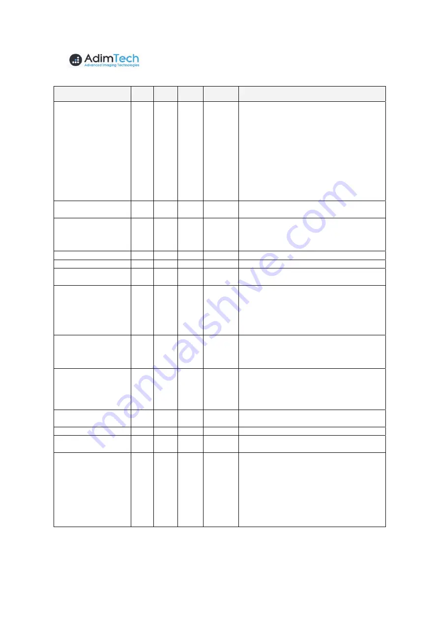
Parameter
Parameter
R/W
Offset
(byte)
Size
(byte)
Value
after start
Description
ADC_TEST_MODE R/W
32 4
EEPROM
Each byte controls the mode of one ADC, first
is ADC 1. The codes in the lower 3 bits are:
0: Normal measurement
1: 10 0000 0000 0000
2: 11 1111 1111 1111
3: 00 0000 0000 0000
4: 10 1010 1010 1010, 01 0101 0101 0101
5: Long pseudorandom
(See Sect. 5.6 of
ITU-T 0.150 (05/96) standard )
6: Short pseudorandom
(See Sect. 5.1 of
ITU-T 0.150 (05/96) standard )
7: 11 1111 1111 1111, 00 0000 0000 0000
FACTORY_RESET W 37 1
N/A
Writing hex CD into this register causes all
settings to return to factory reset.
BYTE_PER_SAMPLE R
40
4
N/A
The ADC indicates here the number of bytes
per sample sent in one stream. The four bytes
correspond to the four streams, (See section
2.6)
CLOCK_PLL_MULT R/W
46 1
EEPROM
External clock PLL multiplier. Valid: 2..33
CLOCK_PLL_DIV R/W
47
1
EEPROM
External clock PLL divider. Valid: 1..32
OFFSET R/W
48
64
EEPROM
These are the 32x2byte offset settings for the 32
analog channels. Standard values are 500..1000.
INT_TRIG_LEVEL R/W
112
64
EEPROM
32x2 bytes internal trigger setting for each
channel:
Bits 0...13: trigger level
Bit 14: 0: positive trigger (level)
1: negative trigger (level)
Bit 15: Enable trigger from this channel
ACT_SAMPLE R
176
16
0
4x4 byte indicating the number of acquired
samples per stream. As the sample timing is
identical for all channels these values are nor-
mally identical.
OVERLOAD_LEVEL R/W 192 2
EEPROM
Overload condition setting for all channels:
Bits 0...13: level
Bit 14: 0: overload above level
1: overload below level
Bit 15: Overload enable.
OVERLD_STATUS R/W
194
1
0
Bit 0: overload status
Writing this register clears overload.
OVERLD_TIME R/W
195
2
EEPROM
Overload time in 10 µs units.
TRIGGER_DELAY R/W
197
4
EEPROM
Delay of data transmission start after any trigger
condition in units of the base clock period time.
FILTER_COEFF R/W
208
16
EEPROM
Signed 16 bit integer coefficients for digital
filter. These should be written sequentially, they
are loaded into the FPGA when the last byte is
written.
Order of 2-byte coefficients:
COEFF_01...COEFF_05: FIR coefficients
COEFF_06: Recursive filter coefficient.
COEFF_07: Reserved
Coeff_08: Filter divide factor: 0...11.
Table 6. Register table of theDAQ unit, part two.