AXM-
A75 User’s Manual
Multifunction I/O Mezzanine Board
_____________________________________________________________________________________
- 17 -
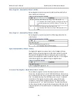
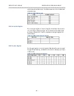
Table 3-8 ADC Clock Period
Module
Clock Period
PMC-LXxxx
10.101 ns
PMC/XMC-SLXxxx, PMC/XMC-VxXxxx,
8 ns
XMC-SLX-150(-1M)
20 ns
XMC-7A200, XMC-7KxxxAX
10 ns
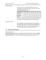
Table 3-9 Conversion Timer 8110H
BIT
FUNCTION
31
–
0
Sample Period = register value * ADC Clock Period
FLASH Data Register - (Read/Write, P 8114H)
A byte write to this address triggers a write/read serial transfer
to/from the serial FLASH device. A byte read from this address
returns the data read from a previous write/read serial transfer.
WARNING: Factory calibration data is stored in FLASH. Writing to
FLASH could result in loss of factory calibration data. See
Error! R
eference source not found.
.
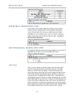
Table 3-10 FLASH Data Register 8114H
BIT
FUNCTION
31 - 8
unused
7 - 0
FLASH data
Digital I/O Direction Register - (Read/Write, P 8118H)
The Digital I/O Direction provides an output enable for each of the 16
digital I/O lines. Write a ‘1’ to a bit to enable the output.
Table 3-11 Digital I/O 8118CH
BIT
FUNCTION
31 - 16
unused
15 - 0
Digital I/O Direction [15 .. 0]
0
–
input
1
–
output
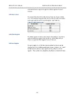
ADC Channels
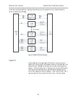
There are three registers associated with each of the sixteen ADC
channels: data, gain correction, and offset correction. The data
register is a 16-bit read only register. Reading this register will
retrieve the oldest value from the FIFO associated with that channel.
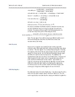
Each of the ADC channels will apply a gain and offset correction to
each sample prior to writing the result to a FIFO. The addition and
multiplication operations are done in FPGA hardware using one of the
FPGA’s DSP blocks for each channel.
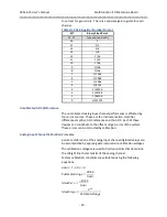
The gain and offset registers are
set to one and zero respectively upon reset to pass uncorrected ADC
values to the FIFOs. Typical start-up operation would include reading
factory calibration constants from AXM-A75 on-board FLASH memory
and writing the appropriate correction values for the currently


