PCIe Accelerator-6D Card User Guide (UG074)
Speedster FPGAs
33
Chapter - 5: PCIe Accelerator-6D Card Clocking
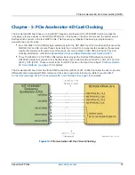
The Accelerator-6D board has an on-board IDT frequency synthesizer U12 (8T49N287) which provides the
necessary reference clocks to the HD1000 FPGA PLL clock banks on the four corners and the bottom select
SerDes which connect to the four QSFP ports. This frequency synthesizer has been pre-programmed to
generate two sets of clocks:
Four 100 MHz 1.8V LVCMOS single-ended clocks for the HD1000's four PLL clock banks that are on the
NW, NE, SW and SE corners.These clocks help the on-chip PLL to generate the necessary frequencies
required to implement the system-level functions. For more details on HD1000 clock bank PLLs and
clocking architecture, refer to the
Speedster22i Clock and Reset Networks User Guide (UG027)
Three 156.26 MHz 3.3V LVPECL differential clocks provide the SerDes PMA reference clocks to
HD1000's bottom four groups of four SerDes lanes each (bottom SerDes CH0 [8:11], CH1 [16:19], CH2
[24:27], CH3 [28:31). These connect to the four QSFP ports on the board. See figure,
for details.
6D Card Interfaces, (see page 18)
The Accelerator-6D board also has three SMP connectors (J3000, J3001, J3002) that allow the user to provide
differential and single-ended FPGA reference clocks via an external clock source. Refer to section
for details.
PCIe Accelerator-6D Card Interfaces (see page 18)
Figure 14:
PCIe Accelerator-6D Rev C Board Clocking
Save


