background image

 57

Part list 

No. 

Photo 

Part Name 

Part No. 


Hinge Cover 

FAAA6932000 

Base Assy 

FAAA691D000 


Rear Cover 

FAAA6914000 

Base FAAA691C000 


Neck FAAA6921000 

Summary of Contents for AL1916

Page 1: ... 1 Acer AL1916p Service Guide Service guide files and updates are available on the CSD web for more information Please refer to http csd acer com tw ...

Page 2: ...ect to the contents hereof and specifically disclaims any warranties of merchantability or fitness for any particular purpose Any Acer Incorporated software described in this manual is sold or licensed as is Should the programs prove defective following their purchase the buyer and not Acer Incorporated its distributor of its dealer assumes the entire cost of all necessary servicing repair and any...

Page 3: ...ing To better fit local market requirements and enhance product competitiveness your regional office MAY have decided to extend the functionality of a machine e g add on card modem or extra memory capability These LOCALIZED FEATURES will NOT be covered in this generic service guide In such cases please contact your regional offices or the responsible personnel channel to provide you with further t...

Page 4: ...ed to try to correct the interference by one or more of the following measures 1 Reorient or relocate the receiving antenna 2 Increase the separation between the equipment and receiver 3 Connect the equipment into an outlet on a circuit different from that to which the receiver is connected 4 Consult the dealer or an experienced radio TV technician for help Warning Use only shielded signal cables ...

Page 5: ...ur home consult your dealer or local power company z The monitor is equipped with a three pronged grounded plug a plug with a third grounding pin This plug will fit only into a grounded power outlet as a safety feature If your outlet does not accommodate the three wire plug have an electrician install the correct outlet or use an adapter to ground the appliance safely Do not defeat the safety purp...

Page 6: ...ay find slightly uneven brightness in the screen depending on the desktop pattern you use z The LCD screen has effective pixels of 99 99 or more It may include blemishes of 0 01 or less such as a missing pixel or a pixel lit all of the time z Due to the nature of the LCD screen an afterimage of the previous screen may remain after switching the image when the same image is displayed for hours In t...

Page 7: ...RICAL SPECIFICATION 35 SAFETY 37 Chapter 2 Operating Instruction 39 CONTROLS 39 MAIN OSD MENU 40 OSD MESSAGE 42 PLUG AND PLAY 44 WHITE COLOR TEMPERATURE 45 AUDIO TECHNICAL SPECIFICATION 45 Chapter 3 Machine Disassembly and Replacement 47 DISASSEMBLY PROCEDURE 47 Chapter 4 Troubleshooting 50 TROUBLESHOOTING 54 Chapter 5 Connector Information 55 CONNECTOR INFORMATION 58 Chapter 6 FRU List 59 PART LI...

Page 8: ...atest LCD technology to provide a performance oriented product with no radiation This will alleviate the growing health concerns It is also a space saving design allowing more desktop space and comparing to the traditional CRT monitor it consumes less power and gets less weight in addition MTBF target is 20k hours or more Comparison Chart of AL1916 AA698T AA698A Panel Normal 19 panel AU M190EN04 V...

Page 9: ...ontrol In the center unless otherwise specified Power input 110Vac or 230Vac Ambient temperature 20 5 C 68 9 F Analog input mode 1280 x1024 60 Hz MEASUREMENT SYSTEMS The units of measure stated in this document are listed below 1 gamma 1 nano tesla 1 tesla 10 000 gauss cm in x 2 54 lb kg x 2 2 degrees F C x 1 8 32 degrees C F 32 1 8 u 4x 2x 12y 3 v 9y 2x 12y 3 x 27u 4 9u 2 12v 9 y 3v 9u 2 12v 9 ni...

Page 10: ...ng 300 typical AU 270 typical Response time Tr Tf LG Ta 25 C 2 10ms typical Samsung Ta 25 C 1 7 6 3ms typical AU Ta 25 C 5 6 2 4ms typical Display color LG 16 2M color with FRC Samsung 16 7M AU 16 2M color with FRC Viewing angle CR 10 LG L R 70 70 U D 70 70 Samsung L R 75 75 U D 75 60 AU L R 70 70 U D 75 60 Luminance Uniformity LG 1 3 max Samsung 25 max AU 70 min ...

Page 11: ...VDD 5V fv 60 Hz fDCLK 54 MHz IL 7mArms Item Symbol Condition Min Typ Max Unit Note Contrast Ratio Center of screen CR 350 550 1 2 4 BM 5A Rising TR 5 6 8 4 Response Time Falling TF 2 4 3 6 msec 1 3 BM 7 Luminance of White Center of screen YL 215 270 cd m2 5 BM 5A Rx 0 634 Red Ry 0 354 Gx 0 287 Green Gy 0 621 Bx 0 138 Blue By 0 077 Wx 0 313 Color Chromaticity CIE 1931 White Wy Normal φ 0 θ 0 Viewin...

Page 12: ...Arms Item Symbol Condition Min Typ Max Unit Note Contrast Ratio Center of screen CR 450 700 1 2 4 BM 5A Rising TR 1 7 3 Response Time Falling TF 6 3 9 msec 1 3 BM 7 Luminance of White Center of screen YL 250 300 cd m2 5 BM 5A Rx 0 640 Red Ry 0 329 Gx 0 300 Green Gy 0 600 Bx 0 150 Blue By 0 060 Wx 0 313 Color Chromaticity CIE 1931 White Wy Normal φ 0 θ 0 Viewing Angle TYP 0 03 0 329 TYP 0 03 1 4 PR...

Page 13: ...se time Sum of TR TF Note 4 After stabilizing and leaving the panel alone at a given temperature for 30 min the measurement should be executed Measurement should be executed n a stable windless and dark room 30 min after lighting the back light This should be measured in the center of screen Dual lamp current 13 0mA 6 5mA x2 Refer to the note 1 in the page 14 for more information Environment condi...

Page 14: ...Bmax Bmax Maximum brightness Bmin Minimum brightness Notes 7 Definition of Flicker level Flicker Voltage pp F x 100 LMD Voltage dc One maximum value of three estimated values For this test an LMD Light Measurement Device is needed with adequate response time to track any visible rate flicker component and with a voltage level output proportional To luminance intensity Test Pattern For dot inversio...

Page 15: ...e proper value for the background level Look for shadowing in any direction from box E Independently vary the gray level or color of the background and box E until the worst case shadowing is observed This defines the background Gbkg and foreground Gfg levels to be maintained for the remainder of the test One point only the target will be measured To determine that point proceed as follows Using t...

Page 16: ...ure align the LMD to the center of the Btgt Turn off Btgt With Gbkg set to its proper level measure the luminance or color Next turn on the source box Bsrc Again measure at the center point of Btgt without Btgt present In this case the LMD will be measuring the shadowing level Lsh Panel Relative Humidity JP777 E02 Input Signals Video input Type Analog R G B Input Impedance 75 ohm 2 Polarity Positi...

Page 17: ...he following frequency range is generalized by supported timing If the entered mode does not match the supported timing the display optimization will not be assured Horizontal Frequency 24KHz 80KHz Vertical Frequency 49Hz 75Hz ...

Page 18: ...88 40 VESA 600 60Hz 60 317 628 600 4 1 23 800x600 48 077 1040 800 120 56 64 50 VESA 600 72Hz 72 188 666 600 6 37 23 800x600 46 875 1056 800 80 16 160 49 5 VESA 600 75Hz 75 625 600 3 1 21 1024x768 48 363 1344 1024 136 24 160 65 XGA 60 004 806 768 6 3 29 1024x768 53 964 1328 1024 176 16 112 71 664 COMPAQ XGA 66 132 816 768 4 8 36 1024x768 56 476 1328 1024 136 24 144 75 VESA 768 70Hz 70 069 806 768 6...

Page 19: ...resh rate mode as emergency mode Monitor should display Out of Range warning menu at this mode Video input Connector Analog Video input Connector 15pins mini D Sub Table 2 4 5 Pin assignment for D sub connector PIN NO Separate Sync 1 RED VIDEO 2 GREEN VIDEO 3 BLUE VIDEO 4 GROUND 5 GROUND 6 RED GROUND 7 GREEN GROUND 8 BLUE GROUND 9 PC5V 5V DDC 10 CABLE DETECTION 11 GROUND 12 SDA 13 H SYNC 14 V SYNC...

Page 20: ...X2 10 TX1 18 TX0 3 Shield TX2 TX4 11 Shield TX1 TX3 19 Shield TX0 TX5 4 NC 12 NC 20 NC 5 NC 13 NC 21 NC 6 DDC Serial Clock 14 5V power 22 Shield TXC 7 DDC Serial Data 15 Ground 5V 23 TXC 8 No Connect 16 Hot plug detect 24 TXC In case the power of the PC unit is switched off and the power of the monitor is switched on no voltage may occur at pin 14 Color of plastic parts Blue PC99 ...

Page 21: ...board key board and internal adapter which house the flat panel control logic brightness control logic and DDC The inverter board will drive the backlight of panel and the DC DC conversion The Adapter will provide thr 12V DC power to inverter power board Power board include AC DC inverter ...

Page 22: ... 22 BLOCK DIAGRAM System Block Diagram 1 ...

Page 23: ... 23 2 ...

Page 24: ... 24 3 ...

Page 25: ...24LC21A CN1 D SVB 15 PIN U2 24LC21A CN2 DVI D 24 PIN U3 TSU56AJ or TSU16AJ CN3 E T 96113 0803 U4 MX10E8050IAQC CN5 P TWO AFN300 N2G1Z 30P U5 MAX810 CN6 E T 4500 10 U6 24LC16B CN7 E T 4500 03 U7 APM4461 CN8 E T 96113 1103 U8 APL1085 33CE U9 APL1117 1 8V U10 LM4838 ...

Page 26: ...L Component U3 SN74LVC14 CN1 D SVB 15 PIN U4 NT68F633 CN3 E T 96113 0803 U5 24LC16B CN9 E T 4500 10 U6 NT68521 CN301 E T 96113 1103 U10 APL1085 33CE CN302 E T 4500 03 U13 APL1117 2 5 J1 P TWO AFN300 N2G1Z U14 SI9435 U501 LM4838 ...

Page 27: ... 27 Software flow chart ...

Page 28: ...By changing these settings the picture can be adjusted to your personal preferences z The power cord should be connected z Connect the video cable from the monitor to the video card z Press the power button to turn on the monitor position The power indicator will light up External Controls 1 Auto Adjust Key Exit 4 MENU ENTER 2 5 LED 3 6 Power Key ...

Page 29: ...ct one end of the signal cable to the LCD Monitor s VGA port z Connect the other end of the signal cable to the VGA port on your PC z Make sure connections are secure Connecting the AC Power z Connect the power cord to the LCD Monitor z Connect the power cord to an AC power source ...

Page 30: ...between front bezel and back cover shall be within specification Top and Bottom Left and Right Back cover Bezel concavity Back cover Bezel concavity 0 8mm A 1 3 mm 0 8mm A 1 3 mm Back Cover Hinge Cover concavity 0mm B 0 5mm ...

Page 31: ... 31 Base Neck concavity 0mm C 0 6mm Top and Bottom Left and Right Back cover Bezel step Back cover Bezel step 0mm D 0 8 mm 0mm D 0 8 mm ...

Page 32: ... 32 LCD Horizontally The angle between front bezel and LCD unit in bottom side should not large than 1 0mm The distance of the LCD display unit from left side to right should not large than 4 0mm ...

Page 33: ...S Back Cover PC ABS The Others ABS 94HB For MPRII Front Bezel ABS 94V 0 Back Cover ABS 94V 0 The Others ABS 94HB GAP Spec Gap between panel with bezel is 0 mm gap 1 5 mm Swivel title noise spec When adjust the monitor angle the range should be limited 5º 15º and it should not have any noise ...

Page 34: ...ess adjustment Burst mode Protection function auto recovery type Interface Signals Input 1 AC Inlet HUAJIE SA 4S 066 or compatible 2 J701 SC SCJ 0345 1 X 9 3 6D BLU 3P or compatible Output Connector Pin Assignment 1 The connecter was pitch 2 0mm PIN NO Function Function 1 5Vaudio Audio power optional 2 GND Audio ground 3 GND Ground 4 GND Ground 5 Vbri Brightness control from logical board 0V to 3 ...

Page 35: ...C Electrical specification 3 4 1 1 Input Specification No Item Condition Min Typ Max Unit 1 Input Voltage 100 240 Vac 2 Input requency 47 63 Hz 3 Input Current 1 0 Arms Cold Start Vin 100Vrms 30 A0 P 4 Inrush Current Cold Start Vin 240Vrms 50 A0 P 5 Hold Up Time full load 100Vac input 10 ms 6 Turn on time Vin 110Vac 1 0 S 7 Efficiency Full load 70 8 Consumption Vin 240Vac no load 1 W ...

Page 36: ... Power line on off 5 5Vdc load regulation test the 15Vinv loading at 2 0A 15Vinv load regulation test the 5Vdc loading at 1 5A 3 4 1 3 Protection function 1 SCP Short circuit protection must be acted on both outputs 2 OPP Should be protected when output power consumption is within 60W 75W Inverter Electrical Specification For Samsung LTM190EX Condition Min Typ Max Unit Input Voltage 15 V Input Cur...

Page 37: ...y Vin 15V 80 Operating Life Time 50000 Hr The open lamp voltage is testes at output connector terminal SAFETY Leakage Current 0 25mA 100Vac Insulation Resistance more than 3M ohms while withstanding a voltage of 500Vac Hi Pot 3Kvac with using 3mA cut off current ...

Page 38: ...ED 5S Switch off 3 W Dark LED SYNC On means Normal operation SYNC Off means H sync F 10KHz duty cycle 25 V sync F 10Hz duty cycle 25 CONNECTORS CONTROLS Connectors Power Monitor rear side AC Inlet Analog RGB Monitor rear side Data Cable 15 pin D sub female male Pin Assignment of 15 pin D sub 1 Red Video 9 5V FOR DDC 2 Green Video 10 Detect 3 Blue Video 11 Serial Data for ISP 4 Serial Clock for ISP...

Page 39: ...S Control panel monitor front panel 1 Power ON OFF switch push to ON and push to OFF toggle switch 2 Power LED will be green when monitor is on be amber when in power saving mode 3 Function select 4 Adjust increase 5 Adjust decrease 6 Auto adjust ...

Page 40: ...0 100 Do Auto Config Clock Adjust picture Clock to reduce Vertical Line noise 0 100 Do Auto Config H Position Adjust the horizontal position of the picture 0 100 Do Auto Config V Position Adjust the verticalposition of the picture 0 100 Do Auto Config Warm N A Recall Warm Color Temperature from EEPROM N A Cool N A Recall Cool Color Temperature from EEPROM N A The Color Temperature will be set to C...

Page 41: ...display language to Japanese N A The Language will be set to English H Position Adjust the horizontal position of the OSD 0 100 50 V Position Adjust the verticalposition of the OSD 0 100 50 OSD Timeout Adjust the OSD timeout 10 120 10 Auto Config N A Auto Adjust the H V Position Focus and Clock of picture N A N A N A Source Change Analog and Digital source change option N A N A Information N A Sho...

Page 42: ...ort range will show this message This message will be flying Cable Not Connected When the video cable is not connected will show this message This message will be flying No Signal When the video cable is connected but the is no active signal input will show this message then enter power saving LOGO When the monitor is power on the LOGO will be showed in the center Item of Factory menu Vendor may c...

Page 43: ...o adjust is depends on hardware Adjusted value of R G B gain shall be used for initial value of Contrast in user menu All value shall be adjustable manually This function shall be located in 3 tag of Factory menu 3 Factory color temp data edit Following data for color temp shall be editable manually color temp default preset No ...

Page 44: ...esent When there is no video input signal this monitor following a time out period will automatically switch to an OFF mode This reduces the monitor s internal power supply consumption After the video input signal is restored full power is restored and the display is automatically redrawn The appearance is similar to a Screen Saver feature except the display is completely off The display is restor...

Page 45: ... 03 0 198 0 469 u v 0 01 User TCO 0X A 2 6 1 requirement User should follow Microsoft Windows Color Quality Specification for Liquid Crystal Display OEM s http www microsoft com hwdev tech color ColorTest asp Audio Technical specification General Description Output power 1W 1W maximum Total harmonic distortion Less than 1 except speakers distortion Input signal sensitivity 0 5 Vrms for full output...

Page 46: ... Audio Voltage Gain 500m Vrms 1KHz 6 d B Volume Max load 4 Ω Frequency Response 500m Vrms 300Hz 20KH z 10dB 10d B Volume Max load 4 Ω Signal to Noise ratio 500m Vrms 1KHz 40dB Volume Max load 4 Ω Total harmonic distortion 500m Vrms 1KHz 1 except speakers distortion Cross talk 500m Vrms 1KHz 30dB Volume Max load 4 Ω Output Watt 500m Vrms 1KHz 0 5W Volume Max load 4 Ω Volume Control Analog ...

Page 47: ...hinge 3 Remove the base Disassemble the chassis 1 Remove the four screws to release the back cover 2 Remove the two screws to release the EMI cover from chassis 3 Remove the two screws from VGA connector 4 Then take the chassis 5 Remove the two screws from bezel 6 To separate the chassis and bezel 7 Remove the four screws from chassis and release the panel ...

Page 48: ...e three screws from Chassis and release the main board Disassemble the power board 1 Disassemble two voltage lines from power board 2 Remove the one screw to release line from Chassis 3 Remove the three screws from Chassis 4 Remove the two screws to release power board from Chassis 5 Then take the power board from the chassia Disassemble the key board 1 Remove the one screw to release VK board fro...

Page 49: ...49 Disassemble the speakers 1 Remove the two screws to release line and VK board from bezel 2 Remove the two screws to release line and chassis from bezel 3 Remove the four screws from bezel ...

Page 50: ...50 Chapter 4 Troubleshooting Main Procedure ...

Page 51: ...51 Power Circuit and Backlights Troubleshooting ...

Page 52: ...52 Performance Troubleshooting ...

Page 53: ...53 Function Troubleshooting ...

Page 54: ...nnector Analog Video input Connector 15pins mini D Sub Table 2 4 5 Pin assignment for D sub connector PIN NO Separate Sync 1 RED VIDEO 2 GREEN VIDEO 3 BLUE VIDEO 4 GROUND 5 GROUND 6 RED GROUND 7 GREEN GROUND 8 BLUE GROUND 9 PC5V 5V DDC 10 CABLE DETECTION 11 GROUND 12 SDA 13 H SYNC 14 V SYNC 15 10 5 1 6 11 15 SCL J1 PHONEJACK STEREO 1 2 3 ...

Page 55: ...om tw spl For whatever reasons a part number change is made it will not be noted in the printed Service Guide For ACER AUTHORIZED CERVICE PROVIDERS your Acer office may have a DIFFERENT part number code to those given in the FRU list of this printed Service Guide You MUST use the local FRU list provided by your regional Acer office to order FRU parts repair and service of customer machines NOTE To...

Page 56: ...56 ...

Page 57: ...57 Part list No Photo Part Name Part No 1 Hinge Cover FAAA6932000 2 Base Assy FAAA691D000 3 Rear Cover FAAA6914000 4 Base FAAA691C000 6 Neck FAAA6921000 ...

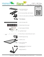
Page 58: ...914A00 8 MB AU 461ACQ30011 SAMSUNG 461ACQ30001 9 Power Board to MB cable AU 453AC530051 Samsung 453AC530051 10 Inverter Board AU 453AC530051 Samsung 453AC530051 11 Front Bezel FAAA6911000 12 Keyboard to MB Cable DCO20191700 ...
Page 59: ...59 13 Frame ECAR9915A00 14 LCD R AC6VA1901R0 AC6VT1901R5 15 Panel to MB cable NBX30001271 NBX30001600 16 Function Board 454AC830001 ...

Page 60: ...N ICS INC V GA INPUT INTERFANCE E DID D sub 2 CA2 3 C C 1 CA1 B AT54C 3 18 MODIFY PCB Name Rev VL922 0A The mark to indicate that Part disuse All Res and Cap size is 0603 R14 1K 1 2 D3 Z 5 6 V 1 2 R2 56 2 1 1 2 R10 100 1 2 R16 10K 1 2 R9 100 1 2 CN 1 D SUB 8 7 6 5 4 3 2 1 9 10 11 12 13 14 15 R13 2 2K 1 2 U1 24LC02 A0 1 A1 2 A2 3 GND 4 VCC 8 WP 7 SCL 6 SDA 5 C11 0 1uF 1 2 R12 1K 1 2 C7 0 047u F 1 2...

Page 61: ... PCB Name Rev VL922 0A The mark to indicate that Part disuse All Res and Cap size is 0603 C93 0 1uF C13 0 1 uF 1 2 R24 10K 1 2 D13 D A 204K 1 2 3 R27 10K 1 2 L6 JKMT_B201209J800TT L0805D 1 2 U2 24LC02 NC 1 NC 2 WP 3 GND 4 VCC 8 WP 7 SCL 6 SDA 5 C N 2 D VI D RX2 1 RX2 2 GND 3 RX4 4 RX4 5 SCL 6 SDA 7 VS 8 RX1 9 RX1 10 GND 11 RX3 12 RX3 13 5V 14 GND 15 HP 16 RX0 17 RX0 18 GND 19 RX5 20 RX5 21 GND 22 ...

Page 62: ... 1uF 1 2 C27 100uF 16V C25 0 1uF 1 2 C32 0 1uF 1 2 C15 0 1uF 1 2 C55 120pF 1 2 C89 N C 100pF 1 2 C33 0 1 uF 1 2 C92 10uF 16V R3 6 1M 1 2 R108 1 5K 1 2 C36 0 1uF 1 2 C17 0 1uF 1 2 C37 22pF 1 2 C30 0 1uF 1 2 C34 0 1uF 1 2 C19 0 1uF 1 2 U3 TSU 56A J RIN0 33 GIN0 30 SOGIN0 31 BIN0 28 RIN0M 32 GIN0M 29 BIN0M 27 HSYNC0 126 VSYNC0 127 R 3 R 4 G 6 G 7 B 9 B 10 CK 12 CK 13 REXT 15 REFP 37 RMID 36 REFM 38 C...

Page 63: ...0603 R P 2 10K 1 2 3 4 5 6 7 8 R50 10K 1 2 U4 Mxic_MX10E8050I A QC P4 2 PWM2 1 P1 0 T2 2 P1 1 T2EX 3 P1 2 4 P1 3 5 P1 4 6 P1 5 7 RST 10 P3 0 RxD 11 P4 3 PWM3 12 P3 1 TxD 13 P3 2 INT0 14 P3 3 INT1 15 P3 4 T0 16 P3 5 T1 17 P3 6 WR 18 P3 7 RD 19 XTAL2 20 XTAL1 21 GND 22 P4 0 PWM0 23 P2 0 A8 24 P2 1 A9 25 P2 2 A10 26 P2 3 A11 27 P2 4 A12 28 P2 5 A13 29 P2 6 A14 30 P2 7 A15 31 PSEN 32 P4 1 PWM1 34 EA 3...

Page 64: ...61 EMITTER COLLECTOR BASE DTC124EK SOT 23B LCD PA NEL POWER CONTROL Main 0805 PCB Name Rev VL922 0A The mark to indicate that Part disuse R88 for current PC B VL 922 rev 0 R89 R90 Q8 f or nest version VL 922 rev 0A R70 0 1 2 R89 10K 1 2 R66 200 R1206D 1 2 R68 33K 1 2 Q6 2SC2411K C50 1000uF 1 0V R69 10K 1 2 R65 10K 1 2 L8 JKMT_B201212K800TM L0805 D 1 2 R85 10K 1 2 R88 0 1 2 C66 10uF Q8 2SC2411K C53...

Page 65: ...5V SOT 223 1206 1206 1206 3 19 Modify PCB Name Rev VL922 0A 0805 C60 0 1uF C69 100uF 16V U9 APL1117 18UC GND 1 OUT 2 IN 3 R79 10K R121 0 R80 NC 0 C65 0 01uF Q4 MMBT3904 1 2 3 C59 220uF 10V C62 0 1uF C64 220uF 10V L11 JKMT_B201212K800TM R72 0 C54 0 1uF C58 220uF 10V R77 1K R71 4 7K C61 0 1uF C71 0 1uF R74 10K L9 JKMT_B201212K800TM U8 APL1084 3 3CE GND 1 OUT 2 IN 3 R78 2 2K R81 0 C73 47uF 16V R84 0 ...

Page 66: ...803 PS104R 1 2 R810 2 7K 1 8W C911 682 X7R C822 102 1KV L803 Bead L701 CHO KE R9 32 3 48K D9 13 BAV99 1 3 2 R938 51K Q801 AP2761I A 1 2 3 R903 10K R9 15 10K W802 R9 13 22 L805 Bead C824 470u f 25V 1 2 R813 1 8 R908 51 1K 1 R804 510K 1206 L704 Bead C921 562 C827 1000u f 10V 1 2 R823 470 1 W R906 100K 1 D914 BAV99 1 3 2 W29 C800 2 22 Y1 U8 00 LTV 817M B R8 09 27K J904 HV 1 LV 2 J905 HV 1 LV 2 C910 1...

Page 67: ... Size Document Nu mber R e v D ate Sheet o f 404AC8 0A SCHEMATIC KEY B VK 922 LAA698 A 3 3 Friday April 29 2005 COMPAL ELECTRONICS INC PCB Name Rev VK922 0 Page_2 The mark to indicate that Part disuse A u to M e nu Power S1 S2 S3 S4 S5 S2 TACK 1 2 S3 TACK 1 2 S5 TACK 1 2 J1 E T 4301 09 1 2 3 4 5 6 7 8 S1 TACK 1 2 S4 TACK 1 2 LED1 LED A1 K A2 ...

Reviews: