ZiLOG S3F8S19 Скачать руководство пользователя страница 22

UM026803-0816

 19

S3F8S19 Development Kit

User Manual

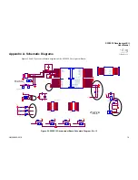
Figure 21. S3F8S19 Development Board Schematic Diagram, #2 of 2
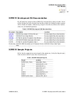
UART CONNECTION

UART CONFIGURATION:

S3F8S19 UART1   R41  R39 (DEFAULT)

Z8F6481 UART0   R40  R38 

UART

PA5_TXD0
PA4_RXD0

VCC_T

Z_DBG
Z_RST

Z_RST

Z_DBG

Z_RST

PD5_TXD1

XOUT

XIN

XOUT

XIN

PD4_RXD1

RxD

S3_RXD1

PA4_RXD0

S3_TXD1

PA5_TXD0

PA6_SCL

PC4_MOSI

PC5_SCK0

PA7_SDA

PC2_SS-

VCC_5V

VCC_T

VCC_T

VCC_T

VCC_5v

S3_TXD1

S3_RXD1

S3_RXD0

S3_TXD0

S3_SDA
S3_SCK
S3_MOSI
S3_SCL

S3_SS-
S3_MISO

R38

100 ohm

R17
19.6K

R18
10K

R41

0 ohm

R14

470

Y3

24.000MHZ

R34
3.3K

D7

1N4448W

R19
10K

U3

MIC5318

GND

2

EN

1

IN

3

ADJ

5

OUT

4

BYP

6

Center Pad

7

R20
27

J14

1

C12

0.01uF

C13

4.7uF

J15

1

R21
27

L1
FERRITE BEAD

C11

0.01uF

R39

100 ohm

C14

0.1uF

J12

1

C9

4.7uF

C15

12pF

P1

USB, mini B

VBUS

1

DM

2

DP

3

ID

4

GND

5

SH1

6

SH2

7

SH3

8

SH4

9

h1

10

h2

11

R40

0 ohm

J16

HDR/PIN 2x3

1

2

3

4

5

6

C16

12pF

C8

1uF

C5

4.7uF

C10

0.1uF

R35

4.7K 

R16

20K

1

3

2

J11

1

D5

GREEN

2

1

C7

1uF

Z8F6481AN

U4

PA2

/DE0

/C

LK

2

IN

/X

2I

N

1

PA3

/CT

S0

-/X2

O

UT

2

PE

3

/T

4C

H

A/

ESO

U

T0

3

PD6

/D

E1

4

PA4

/RXD0

/MO

SI0

5

PA5

/TXD

0/

S

C

K

0

6

P

D5

/T

X

D1

7

PA

6

/T

1I

N

/T

1O

U

T-

/S

CL

8

PC4

/MO

SI0

/T0

IN/T0

O

U

T-/SCL

/D

E0

9

P

C5

/SC

K0

/T0

OUT

/S

DA/CTS

0-

10

PA

7

/T

1O

U

T

/S

DA

1

1

PD4/RXD1

12

PC6/T2IN/T2OUT-/SCKOUT/ESOUT0

13

PC7/T2OUT/CTS1-/ESOUT1

14

VDD

15

PD0/RESET-

16

DBG

17

PD3/C1OUT/AMPBOUT/ANA8

18

VSS

19

PC0/ANA4/VBIAS/C0INP

21

PC1/MISO0/ANA5/C0INN

22

PC2

/AN

A3

/SS0

-

23

PC

3/

M

IS

O0

/A

NA

11

/DAC

24

PD2

/C1

IN

P/AM

PBI

N

P/

A

NA6

2

5

P

D1

/C1

INN

/AM

PB

INN/ANA

7

26

PB0

/AN

A0

/AM

PAO

UT

27

PB

1

/A

NA1

/AM

PAINN

2

8

PB

2

/A

NA2

/AM

PAINP

2

9

PB4

/VR

EF+

30

PB3

/VRE

F-

31

PE5

/T4

CHC/

ESO

UT

2

32

PE6

/T4

CHD

/ESO

UT

3

3

3

PE2/T4IN

34

VCORE

35

AVDD

36

VDD

37

PA0/T0IN/T0OUT-/CLKIN/XIN

38

PA1/T0OUT/XOUT

39

VSS

40

AVSS

41

PD7/C0OUT

42

PE1/DM/T0OUT

43

PE0/DP/T0IN/T0OUT-

44

PE4/T4CHB/ESOUT1

20

J20

1
2
3
4
5
6

R15
16.5K

R36

3.3K

C6

0.1uF

R33

4.7K 

Содержание S3F8S19

Страница 1: ...S3 Family of Microcontrollers S3F8S19 Development Kit Copyright 2016 Zilog Inc All rights reserved www zilog com UM026803 0816 User Manual...

Страница 2: ...o perform can be reason ably expected to cause the failure of the life support device or system or to affect its safety or effectiveness Document Disclaimer 2016 Zilog Inc All rights reserved Informat...

Страница 3: ...n To learn more refer to the corresponding page s or appropriate links furnished in the table below Date Revision Level Description Page Aug 2016 03 Updated for ZDS S3 version 5 3 0 Removed ISP I supp...

Страница 4: ...tures an S3F8S19 MCU in a 48 pin QFP package plus an S3 PGM connector to connect the Board to a host development PC using the S3 Flash In System Programmer II ISP To learn more about the S3F8S19 MCU r...

Страница 5: ...al Flash memory and 2 KB of internal RAM memory USB interface to supply power to the board and used as a PC virtual COM port with the S3 Monitor and Boot Loader libraries LCD module Buzzer Speaker UAR...

Страница 6: ...ior to connecting the S3F8S19 Development Board to your development PC down load ZDSII for S3 Family devices version 5 3 0 or later from the Downloadable Software category in the Zilog Store 2 When th...

Страница 7: ...I as shown in Figure 3 3 Connect the other end of the ribbon cable to Jumper J6 on the Development Board Ensure that Pin 1 on the ribbon cable is aligned with Pin 1 on the target connector as indicate...

Страница 8: ...SP II 4 With the USB A male to Mini B cable connect Port P1 on the S3F8S19 Develop ment Board to a USB port on the Development PC to apply power to the Development Board as indicated in Figure 5 After...

Страница 9: ...ing application To start the S3F8S19 Ledblink sample program observe the follow ing procedure 1 Launch ZDSII by navigating from the Windows Start menu to Programs Zilog ZDSII S3 Version ZDSII S3 Versi...

Страница 10: ...er Manual 7 3 Select the ledblink zdsproj project from within the ledblink_asm folder as indicated in Figure 8 and click Open A list of source files will appear in the Work space panel Figure 7 The Op...

Страница 11: ...ug then click OK to close the Select Configuration dialog box 6 From the Project menu in ZDSII select Settings to open the Project Settings dialog box In the Project Settings dialog box click the Debu...

Страница 12: ...ommunication dialog box 10 Make sure that the Enhanced ISP Debug Library is selected 11 Click OK to close the Project Settings dialog box 12 If you are prompted to rebuild any affected files click Yes...

Страница 13: ...19 Ledblink sam ple program Ensure that the LED indicator on the S3 Flash ISP II lights up upon connecting to the USB port of your PC Navigate to Project Settings Debugger Debug Tool Setup Upon click...

Страница 14: ...it is to provide a set of hardware and software tools for the development of hardware and firmware for applications based on the S3F8S19 microcontroller An image of the S3F8S19 Development Board is sh...

Страница 15: ...on stabilization control or watch dog timer function One 16 bit timer counter Timer 0 with Interval mode and PWM mode Table 1 Operations and Power Options of the S3F8S19 Development Board Option Opera...

Страница 16: ...on ROM address 3FH via Smart Option To learn more about the S3F8S19 MCU refer to the S3F8S19 S3F8S15 Product Specifi cation PS0312 Magnetic Buzzer The CEM1206S magnetic buzzer U2 manufactured by CUI I...

Страница 17: ...s circuit resets the S3F8S19 MCU when SW1 is pressed See Figure 15 for a representation of the reset cir cuit ISP II Connector The ISP II connector J6 provides an interface between the S3 Flash ISP II...

Страница 18: ...aritronix Ltd is a 20 pin module seated on both J4 and J5 Figure 17 shows an image of this LCD This four digit LCD is activated by selecting the segment of each digit that must light up Figure 18 show...

Страница 19: ...der Utility A Flash Loader utility is included in Zilog Developer Studio II via the Tools menu Figure 19 shows an image of the Flash Programming screen You can program the S3F8S19 MCU directly using t...

Страница 20: ...S3F8S19 Development Kit Documentation Document Description Location UM0268 S3F8S19 Development Kit User Manual Documentation Tools_Documentation PS0312 S3F8S19 Product Specification Documentation Chi...

Страница 21: ...4 U2 S3F8S19 QFP P0 4 ADC4 1 P0 3 INT3 ADC3 2 P0 2 INT2 ADC2 3 P0 1 INT1 ADC1 SDAT 4 P0 0 INT0 BUZ ADC0 SCLK 5 VDD 6 VSS 7 Xout 8 Xin 9 TEST VPP 10 XTin 11 XTout 12 RESET 13 P2 0 COM0 14 P2 1 COM1 15...

Страница 22: ...SH1 6 SH2 7 SH3 8 SH4 9 h1 10 h2 11 R40 0 ohm J16 HDR PIN 2x3 1 2 3 4 5 6 C16 12pF C8 1uF C5 4 7uF C10 0 1uF R35 4 7K R16 20K 1 3 2 J11 1 D5 GREEN 2 1 C7 1uF Z8F6481AN U4 PA2 DE0 CLK2IN X2IN 1 PA3 CTS...

Страница 23: ...og s Technical Support page at http support zilog com To learn more about this product find additional documentation or to discover other fac ets about Zilog product offerings please visit the Zilog K...

Отзывы: