


4-4
DECK MECHANISM DISASSEMBLY
2. Plate Top (Fig. A-2-1)
1) Pull the (B) portion of the Plate Top back in direction of
arrow and separate the right side of it.
2) pull the (B’) portion of the Plate Top back in direction of
arrow and separate the left side of it.
(Used tools : (-) type driver, anything tool with sharp
point or flat point.)
NOTE
(1) When reassembling, push the Plate Top after alignment
the two position(C), (C’) as below Fig.
3. Holder Assembly CST (Fig.A-2-2)
1) Move the Holder Assembly CST in direction of arrow and
separate the left side of it first through the (D) position of
the Chassis.
2) Disassemble the right side of the Holder Assembly CST
from each guided hole of the Chassis.
NOTE
When reassembling, insert the (E) part of the Holder
Assembly CST in the (E’) hole of the Chassis first and
assemble the left side of it.
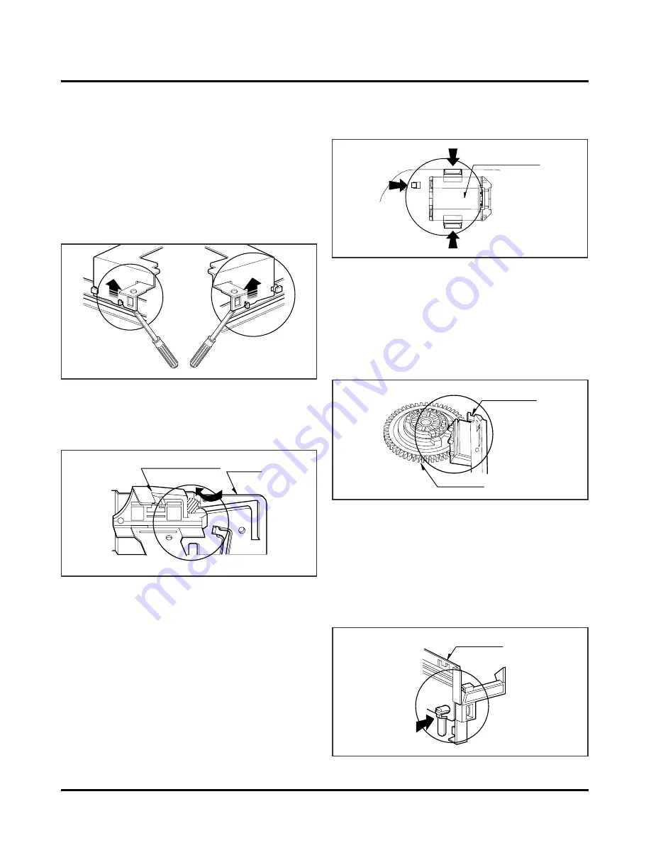
4. Opener Door (Figure. A-2-3)
1) Turn the Opener Door clockwise and remove it through
the guide hole of the Chassis.
5. Bracket Assembly L/D Motor
(Fig. A-2-4)
1) Unplug the Connector(C1).
2) Unhook three Hooks(H3, H4, H5) on bottom side of the
Chassis, lift up the Bracket Assembly L/M and disassem-
ble the Bracket Assembly L/D Motor.
6. Gear Assembly Rack F/L (Fig. A-2-5)
1) Move the Gear Assembly Rack F/L in direction of
arrow(A) and unhook the Hook(H6) pulling back in front.
2) Separate the Gear Rack F/L in direction of arrow(B).
NOTE
When reassembling, align the gear part of the Gear
Assembly Rack F/L with the Gear Drive as below Fig.
7. Arm Assembly F/L (Fig. A-2-6)
1) Move the Arm Assembly F/L in direction of arrow and
separate the left side of it first.
2) Disassemble the Arm Assembly F/L from each guided
hole of the Chassis.
8. Lever Assembly S/W(Fig. A-2-7)
1) Unhook the Hook(H8) in the left side of the Chassis and
remove the Lever Assembly S/W.
(B')
(C')
(C)
(B)
(D)
Holder assembly CST
Chassis
Gear Rack F/L
Gear Drive
(H8)
Chassis
(H3)
(H4)
(H5)
Bracket assembly L/M
Содержание XBS344 Series
Страница 2: ......
Страница 10: ...2 3 951 954 960 961 953 957 959 955 956 963 A90 2 Woofer Speaker Section DTE 5105WE...
Страница 11: ...2 4 850 852 851A 851 853 854 857 858 A80 3 Speaker Section DTE 550TE...
Страница 38: ...3 34 3 35 2 POWER SMPS CIRCUIT DIAGRAM 2 SR13601A R171 4 7K...
Страница 39: ...3 36 3 37 3 JACK TUNER CIRCUIT DIAGRAM 03 08 15 SR13605A...
Страница 43: ...3 44 3 45 7 KEY CIRCUIT DIAGRAM SR13610A...
Страница 46: ...3 50 3 51 PRINTED CIRCUIT DIAGRAMS 1 MAIN P C BOARD LOCATION GUIDE...
Страница 47: ...3 52 3 53 2 TUNER P C BOARD LOCATION GUIDE 3 POWER P C BOARD...
Страница 48: ...3 54 3 55 4 KEY 1 LEFT P C BOARD LOCATION GUIDE 5 KEY 2 RIGHT P C BOARD LOCATION GUIDE...
Страница 49: ......
Страница 69: ...3 75 3 C IC507 PIN 26 FIG 12 3 2 Y IC507 PIN 21 FIG 12 2...
Страница 77: ......
Страница 79: ...CD DVD LD will not on SR13608A VZ DV51V SANYO 3 85 3 86 2 RF SERVO CIRCUIT DIAGRAM...
Страница 80: ...VZ DV51V SANYO TUNER_L TUNER_R 3 87 3 88 3 AUDIO _COM CIRCUIT DIAGRAM DVD AMP...
Страница 81: ...VZ DV51V SANYO FRONT_R FRONT_L REAR_R REAR_L 3 89 3 90 4 DIGITAL AMP CIRCUIT DIAGRAM DVD AMP...
Страница 82: ...5 PWM CODEIC CIRCUIT DIAGRAM DVD AMP VZ DV51V SANYO 12 288MHz R R L L R L OPTICAL_IN 3 91 3 92...
Страница 83: ...6 INTERFACE CIRCUIT DIAGRAM DVD AMP VZ DV51V SANYO 3 93 3 94...
Страница 86: ...LOCATION GUIDE LOCATION GUIDE 3 99 3 100 PRINTED CIRCUIT DIAGRAMS 1 DVD AMP P C BOARD...
Страница 87: ......
Страница 119: ...MEMO...
Страница 125: ......
Страница 127: ......
Страница 159: ......


