PSR-540
16
14
014: Output R
Connect the level meter (with a JIS-C filter) to the [PHONE/AUX OUT] jack. (33
ohm load)
Set the [MASTER VOLUME] at maximum.
Check the output level (1kHz).
Phones L: Less than -60.0 dBm
Phones R: -10 dBm +/- 2 dB
15
015: Output L
Connect the level meter (with a JIS-C filter) to the [PHONE/AUX OUT] jack. (33
ohm load)
Set the [MASTER VOLUME] at maximum.
Check the output level (1kHz).
Phones L: -10 dBm +/- 2 dB
Phones R: Less than -60.0 dBm
19
019: D/A Noise
Connect the level meter (with a JIS-C filter) to the [PHONE/AUX OUT] jack. (33
ohm load)
Set the [MASTER VOLUME] at maximum.
Phones L/R: Less than -80 dBm
20
020: SW, LED Chk
Check the switches on the panel.
Press the switches that are displayed on the LCD.
A pre-assigned note is output when pressing the switch.
The test results appear on the LCD.
21
021: ALL LED On
Check that the LED on the panel is on.
22
022: Red LED On
Check that the red LED on the panel is on.
23
023: Green LED On
Check that the green LED on the panel is on.
28
028: All LCD On
Check that all LCD dots are on.
29
029: All LCD Off
Check that all LCD dots are off. The LCD becomes white
31
031: Pedal1 Chk
Connect the foot switch to the [FOOT SWITCH] jack.
Check that the C3 note is output when starting the test program.
Check that the C4 note is output when pressing the pedal and that the tone is
turned off when releasing the pedal.
The test results appear on the LCD.
37
037: Midi Chk
After connecting the [MIDI IN] jack and [MIDI OUT] jack with a MIDI cable, ex-
ecute the test.
Check that the C4 note is output and that the test results appear on the LCD.
38
038: To Host Chk
For factory test use only
40
040: Battery Chk
Checks the voltage of the Battery terminal
41
041: Rom Chk2
Checks the ROM
The test results appear on the LCD.
42
042: Ram Chk2
Checks the RAMs that are connected to the CPU.
The test results appear on the LCD.
43
043: WaveRom Chk2
Checks the WAVE ROMs that are connected to the CPU.
The test results appear on the LCD.
44
044: WaveRam Chk1
Checks all the WAVE RAMs that are connected to the CPU.
The test results appear on the LCD.
46
046: Backup Chk2
Performa the RAM back-up check.
Check that the display reads “NG,” then turn off the power switch.
Enter the test program and perform the RAM back-up checks, then check again.
Check that the LCD displays “OK.”
Note: Do not turn on the power switch by normal mode while standing by, as
the RAM data will be lost.
47
047: Factry Set
All the RAMs are initialized and set to the factory preset date when executing
this test. The results appear on the LCD.
48
048: Test Exit
Exit from the test program after executing this test.
1
001: Version
Displays Rom version
Rom (Program, Wave) versions are displayed alternately on the LCD.
2
002: Rom Chk1
Checks the ROM
The tset results appear on the LCD.
3
003: Ram Chk1
Checks all the RAMs that are connected to the CPU.
The test results appear on the LCD.
4
004: WaveRomChk1
Checks the WAVE ROMs that are connected to the CPU.
The test results appear on the LCD.
7
007: FDD Chk
Insert the floppy disks one by one (2DD and 2HD).
Checks the floppy disk drive unit
9
009: Eff1Ram Chk
Checks the effect RAM1
11
011: TG1 Chk
Outputs the sine wave by changing the channels in sequence from C2 to G4.
After auto-scaling is finished, individual keys can be played. (If playing two or
more keys simultaneously, the first pressed key has priority to make a sound.)
13
013: Pitch Chk
Connect the frequency counter to the [PHONE/AUX OUT] jack.
Set PAN to Center and produce a signal at 440 Hz +/- 0.22.
Check that the correct signal is produced.
1. TEST PROGRAM
A. PREPARATION
1)
PA-6 (AC adapter) is used.
2)
The volume is usually moved to the use position when no volume change is required.
3)
Measuring instruments:
Frequency counter
Level meter (with JIS-C filter)
Note: Use a stereo plug to the [PHONES / AUX OUT] jack at 33 ohms.
4)
Jigs:
Foot switch, MIDI cable, Floppy Disk(2HD, 2DD)
B. HOW TO ENTER THE TEST PROGRAM
AUTO MODE
While pressing the C3#, F3 and G3# keys, turn the [STAND BY/ON] switch to the “ON” position.
MANUAL MODE
While pressing the C2#, F2 and G2# keys, turn the [STAND BY/ON] switch to the “ON” position.
C. PROCEEDING THROUGH THE TEST PROGRAM
AUTO MODE
When the test program is started, the test is automatically executed.
When confirmation is necessary, the test program stops operating and waits for instruction. At this time,
press the [START/STOP] button; the next test is automatically executed.
MANUAL MODE
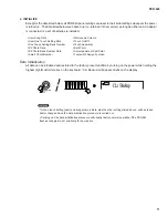
The LCD will display “TEST” when entering the test program.
To select the program number, use the [BANK +] and [NEXT -] buttons.
To execute the test, press the [START/STOP] button.
To proceed to the next test, press the [START/STOP] button.
D. TEST PROGRAM LIST
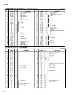
TEST.NO
LCD(initial)
Test functions and Judgement Criteria


