DVR-S60/NX-SW60
55
DVR-S60
NX-SW60
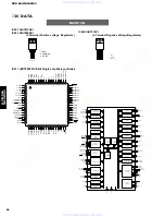
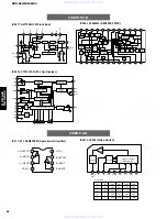
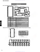
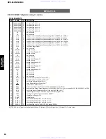
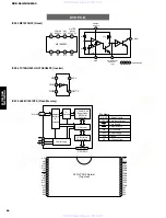
IC806,807 EM636165TS,KM416S1120DT,K4S161622D (1 Mega x 16 Synchronous DRAM)
1
2
3
4
5
6
7
8
9
10
11
12
13
14
50
49
48
47
46
45
44
43
42
41
40
39
38
37
V
SS
DQ15
DQ14
DQ13
DQ12
DQ11
DQ10
DQ9
DQ85
N.C/RFU
V
DD
DQ0
DQ1
V
SSQ
DQ2
DQ3
V
DDQ
DQ4
DQ5
V
SSQ
DQ6
DQ7
V
DDQ
LDQM
15
16
17
18
19
20
21
22
23
24
25
36
35
34
33
32
31
30
29
28
27
26
UDQM
CLK
CKE
N.C
A9
A8
A7
A6
A5
A4
V
SS
V
SSQ
V
SSQ
V
DDQ
V
DDQ
WE
CAS
RAS
CS
BA
A10/AP
A0
A1
A2
A3
V
DD
Pin
Name
Input Function
CLK
System Clock
Active on the positive going edge to sample all inputs.
CS
Chip Select
Disables or enable device operation by masking or enabling all inputs except
CLK,CKE and L(U)DQM
CKE
Clock Enable
Masks system clock to freeze operation from the next clock cycle.
CKE should be enabled at least ono cycle prior to new command.
Disable input buffers for power down in standby.
A0~A10/AP
Address
Row / column addresses are multiplexed on the same pins.
Row address : RA0~RA10, column address : CA0~CA7
BA
Bank Select Address
Selects bank to be activated during row address latch time.
Selects bank for read/write during column address latch time.
RAS
Row Address Strobe
Latches row addresses on the positive going edge of the CLK with RAS low.
Enables row access & precharge.
CAS
Column Address Strobe
Latches column addresses on the positive going edge of the CLK with CAS low.
Enables column access.
WE
Write Enable
Enables write operation and row precharge.
Latches data in standing from CAS, WE active.
L(U)DQM
Data Input/Output Mask
Makes data output Hi-Z, t
SHZ
after the clock and masks the output.
Blocks data input when L(U)DQM active.
DQ0~15
Data Input/Output
Data inputs/outputs are multiplexed on the same pins.
V
DD
/V
SS
Power Supply/Ground
Power and ground for the input buffers and the core logic.
V
DDQ
/V
SSQ
Data Output Power/Ground
Isolated power supply and ground for the output buffers to provide improved noise
immunity.
N.C/RFU
No Connection/
Reserved for Future Use
This pin is recommended to be left No Connection on the device.
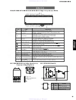
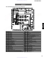
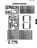
IC811 PQ025EZ01ZPN (Low Voltage Operation Low
1
3
2
5
1
2
3
4
5
Specific IC
1 DC input (V
IN
)
2 ON/OFF control terminal (V
C
)
3 DC output (V
O
)
4 NC
5 GND
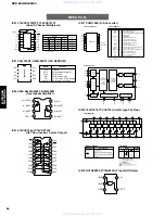
IC812 PST3627UR (Reset IC)
OUT
GND
V
DD
C
D
2
1
GND
1
V
DD
OUT
C
D
2
4
3
3
4
R
D
Vref
PIN No.
1
2
3
4
PIN NAME
GND
V
DD
C
D
OUT
FUNCTIONS
GND Pin
V
DD
Pin / Voltage Detect Pin
Capacitor Connect Pin with Delay
Reset Signal Output Pin
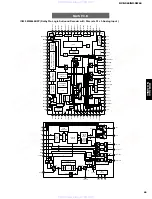
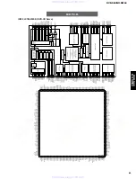
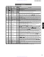
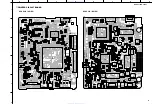
MPEG P.C.B.
www. xiaoyu163. com
QQ 376315150
9
9
2
8
9
4
2
9
8
TEL 13942296513
9
9
2
8
9
4
2
9
8
0
5
1
5
1
3
6
7
3
Q
Q
TEL 13942296513 QQ 376315150 892498299
TEL 13942296513 QQ 376315150 892498299


