background image

CONTENTS

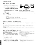
TO SERVICE PERSONNEL .......................................... 2
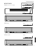
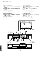
FRONT PANELS ............................................................ 3
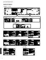
REAR PANELS .............................................................. 4
BOTTOM PANEL ........................................................... 5
REMOTE CONTROL PANELS ...................................... 5
SPECIFICATIONS / 

参考仕様

...................................... 6–7

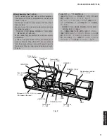
INTERNAL VIEW ........................................................... 7
SET MENU TABLE / 

セットメニュー

.............................. 8

SERVICE PRECAUTIONS / 

サービス時の注意事項

......... 9

DISASSEMBLY PROCEDURES 

/


分解手順

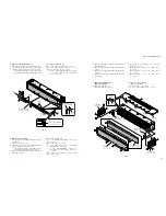
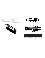
............. 9–17

UPDATING FIRMWARE /

ファームウェアの書き込み

......................................... 18–29

SELF-DIAGNOSTIC FUNCTION /

ダイアグ(自己診断機能)

......................................... 30–51

DISPLAY DATA ........................................................... 52
IC DATA ................................................................. 53–62
BLOCK DIAGRAM ....................................................... 63
PRINTED CIRCUIT BOARDS ................................ 64–75
PIN CONNECTION DIAGRAMS ............................ 76–77
SCHEMATIC DIAGRAMS ...................................... 79–86
REPLACEMENT PARTS LIST ............................ 87–107
REMOTE CONTROL .......................................... 108–110
ADJUSTING SYSTEM PARAMETERS /

拡張メニュー

......................................................... 111–115

1 0 1 0 5 9

SERVICE  MANUAL

DIGITAL SOUND PROJECTOR

 2007                                         All rights reserved.

This manual is copyrighted by YAMAHA and may not be copied or

redistributed either in print or electronically without permission.

P.O.Box 1, Hamamatsu, Japan

 '07.10

YSP-3000/YSP-30D/

HTY-7030

YSP-3000/YSP-30D/

HTY-7030

IMPORTANT NOTICE

This manual has been provided for the use of authorized YAMAHA Retailers and their service personnel.
It has been assumed that basic service procedures inherent to the industry, and more specifically YAMAHA Products, are already
known and understood by the users, and have therefore not been restated.

WARNING:

Failure to follow appropriate service and safety procedures when servicing this product may result in personal
injury, destruction of expensive components, and failure of the product to perform as specified.  For these reasons,
we advise all YAMAHA product owners that any service required should be performed by an authorized
YAMAHA Retailer or the appointed service representative.

IMPORTANT:

The presentation or sale of this manual to any individual or firm does not constitute authorization, certification or
recognition of any applicable technical capabilities, or establish a principle-agent relationship of any form.

The data provided is believed to be accurate and applicable to the unit(s) indicated on the cover.  The research, engineering, and
service departments of YAMAHA are continually striving to improve YAMAHA products.  Modifications are, therefore, inevitable
and specifications are subject to change without notice or obligation to retrofit.  Should any discrepancy appear to exist, please
contact the distributor's Service Division.

WARNING:

Static discharges can destroy expensive components.  Discharge any static electricity your body may have
accumulated by grounding yourself to the ground buss in the unit (heavy gauge black wires connect to this buss).

IMPORTANT:

Turn the unit OFF during disassembly and part replacement.  Recheck all work before you apply power to the unit.

Содержание Digital Sound Projector YSP-3000

Страница 1: ... follow appropriate service and safety procedures when servicing this product may result in personal injury destruction of expensive components and failure of the product to perform as specified For these reasons we advise all YAMAHA product owners that any service required should be performed by an authorized YAMAHA Retailer or the appointed service representative IMPORTANT The presentation or sa...

Страница 2: ...erly insulated from supply circuits Meter impedance should be equivalent to 1500 ohms shunted by 0 15µF Leakage current must not exceed 0 5mA Be sure to test for leakage with the AC plug in both polarities 本機に搭載されているすべての基板およびハンダ付けによる接合 部は無鉛ハンダでハンダ付けされています 無鉛ハンダにはいくつかの種類がありますが 修理時には下記の ような無鉛ハンダの使用を推奨します Sn Ag Cu 錫 銀 銅 Sn Cu 錫 銅 Sn Zn Bi 錫 亜鉛 ビスマス 注意 無鉛ハンダの融点温度は通常の鉛入りハンダに比べ30 40 程度高くなっていますので それぞれのハン...

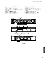
Страница 3: ...0D HTY 7030 YSP 3000 YSP 30D HTY 7030 Top view Front view J model K A G E L V models Top view Front view U C models Top view Front view FRONT PANELS YSP 30D B model HTY 7030 G E models YSP 3000 U C K A G E L V J models ...

Страница 4: ... 30D HTY 7030 REAR PANELS YSP 3000 U C models K model A model G E models L model V model J model YSP 30D B model G E models HTY 7030 YSP 3000 J model YSP 30D B model YSP 3000 U C K A G E L V models HTY 7030 G E models U C A models U C models ...

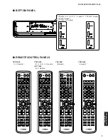
Страница 5: ... YSP 30D HTY 7030 REMOTE CONTROL PANELS YSP 3000 U C models YSP 3000 K A G E L V models HTY 7030 G E models YSP 30D B model YSP 3000 J model BOTTOM PANEL YSP 3000 U C K A G E L V models YSP 30D B model HTY 7030 G E models YSP 3000 J model ...

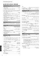
Страница 6: ...site OSD用コンポジット映像信号 U C K V J models NTSC A B G L models PAL Subwoofer PRE OUT HDMI Input Output HDMI入出力 Input DVD AUX1 Output OUT iPod Connection U C A B models DOCK SPECIFICATIONS 参考仕様 IR In U C models Monoral mini jack wired remote control System Connector システム接続 J model Monoral mini jack サブウーファーON OFF連動用 Function Section 機能部 Decode Format デコードフォーマット Dolby Digital Dolby Pro Logic Dolby Pro Logi...

Страница 7: ...Labs Inc TruBass SRSと記号はSRS Lab Inc の商標です TruBass技術はSRS Labs Inc から のライセンスに基づき製品化されています is a trademark of DiMAGIC Co Ltd ユーフォニー はダイマジック社の商標です iPod is a trademark of Apple Inc registered in the U S and other countries The DAB Digital Radio logo and the stylised r mark and Digital One Limited General 総合 Power Supply 電源電圧 U C models AC 120 V 60 Hz K A B G E L models AC 220 240 V 50 60 Hz V model AC 1...

Страница 8: ...100 120 160 200 Hz 20 to 0 dB 0 dB step 0 5 dB 0 3 to 15 0 m 3 0 m step 0 1 m 1 0 to 50 0 ft 10 0 ft step 0 5 ft MUTE 20 dB 0 to 160 ms step 1 ms Maximum changes with the modes 最大値はモードにより変化 SHELF WALL NORMAL HI ECHO MIN STD MAX ON OFF FLAT TO WALL ANGLE TO WALL OR CORNER 2 0 to 12 0 m step 0 1 m 6 5 to 40 0 ft step 0 5 ft 2 0 to 12 0 m step 0 1 m 6 5 to 40 0 ft step 0 5 ft 1 8 to 9 0 m step 0 1 m ...

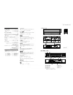
Страница 9: ... during servicing such as wearing insulating gloves Note that positions indicated below are dangerous even after the power is turned off because an electric charge remains and a high voltage continues to exist there Before starting any repair work perform discharge by connecting a discharge resistor 5k ohms 10W between terminals at following positions The time required for discharging is about 30 ...

Страница 10: ...3 screws C Fig 5 b Remove CB501 Fig 5 c Remove power cable together with frame AC Fig 5 d Remove 7 screws D Fig 5 e Remove frame bottom Fig 5 f Remove 6 screws E Fig 5 g Remove CB12 CB504 CB506 and CB507 Fig 5 h Remove POWER 1 P C B Fig 5 6 Removal of INPUT P C B a Remove 4 screws F and 7 screws G Fig 5 b Remove CB6 CB8 CB10 and CB11 Fig 5 c Remove INPUT P C B together with frame input Fig 5 5 POW...

Страница 11: ...sconnected Be sure to use the extension cable before servicing the following section POWER 1 P C B CB506_POWER 2 P C B W901 MF404250 4P 250mm When connecting the flexible flat cable be careful with polarity In this unit the ground of P C B s is connected to the panel or chassis When these P C B s are removed from the panel or chassis connect the ground point to the panel or chassis using a ground ...

Страница 12: ... earth Fig 7 b Remove 3 screws J and then remove flame PCB R Fig 7 c Remove 2 screws K Fig 7 d Remove CB8 Fig 7 e Remove DSP P C B Fig 7 8 Removal of AMP P C B a Remove 5 screws L 4 screws M and then remove flame PCB L Fig 7 b Remove 3 screws N Fig 7 c Remove CB502 510 Fig 7 d Remove AMP P C B Fig 7 7 DSP P C B の外し方 a Hのネジ1本 Iのネジ1本を外し プレートEARTHを 取り外します Fig 7 b Jのネジ3本を外し フレームPCB Rを取り外します Fig 7 c Kの...

Страница 13: ...のネジ8本を外します Fig 9 b グリルネットASSYを取り外します Fig 9 Fig 9 11 Removal of Grille Net Ass y Black color model a Remove 8 screws Y Fig 9 b Remove grille net ass y Fig 9 10 Removal of Front Grille Use full care as you may be injured by the front grille or other part a Remove 6 screws Q Fig 9 b Lift up the rear of the top cover a little and after remov ing 9 hooks remove it rearward Fig 9 To install the top cove...

Страница 14: ...g 12 g Remove driver tweeter Fig 12 Make sure that all the removed driver tweeter parts are reinstalled at specified positions Fig 12 Fig 12 Driver tweeter スピーカユニット ツィーター CB502 CB503 CB504 CB505 CB506 CB507 CB508 TW1 TW3 TW2 TW4 TW6 TW8 TW10 TW12 TW14 TW16 TW18 TW20 TW5 TW7 TW9 TW11 TW13 TW15 TW17 TW19 TW21 a Installation of Driver Tweeter Caution Make sure that all the removed driver tweeter part...

Страница 15: ...本を外します Fig 13 h POWER 4 P C B を取り外します Fig 13 13 Removal of POWER 2 3 and 4 P C B s a Remove 3 screws b Fig 13 b Remove CB903 Fig 13 c Remove POWER 3 P C B Fig 13 d Remove 10 screws c and then remove flame FL Fig 13 e Remove 2 screws d Fig 13 f Remove POWER 2 P C B Fig 13 g Remove 2 screws e Fig 13 h Remove POWER 4 P C B Fig 13 d e d Flame FL フレームFL CB903 POWER 2 P C B POWER 3 P C B POWER 4 P C B b...

Страница 16: ...ヶ所から取り付け 次にネジを取り付け てください Fig 2 Disassembly Procedures as far as Driver Woofer 1 Removal of Top Cover a Remove 6 screws 1 Fig 1 b Lift up the rear of the top cover a little and after remov ing 9 hooks remove it rearward Fig 1 To install the top cover be sure to install 9 hooks at the front first and then install 6 screws 1 Fig 1 2 Removal of Grille Bottom Ass y a Remove 8 screws 2 and 2 screws 3 Fi...

Страница 17: ...イドサブRを取り外しま す Fig 3 e 0のネジ18本を外し フロントグリルを取り外しま す Fig 3 4 グリルネットASSYの外し方 Black color model a Aのネジ8本を外します Fig 3 b グリルネットASSYを取り外します Fig 3 5 スピーカーユニット ウーファー の外し方 a Bのネジ4本 個を外します Fig 3 b スピーカユニット ウーファー を外します Fig 3 3 Removal of Front Grille Use full care as you may be injured by the front grille or other part a Remove 2 screws 4 4 screws 5 and then remove panel side L Fig 3 b Remove 2 screws 6 4 screws...

Страница 18: ...232クロスケーブル Reset switch リセット スイッチ Flexible flat cable 9P カード電線9P Fig 1 5 送信データ ポートを選択します Fig 2 Select Program Internal flash memoryを選択します RS232C 接続しているRS 232Cポートを選択します 5 Select the data to be transmitted and port Fig 2 Select Program Select Internal flash memory RS232C Select the port of RS 232C For selection of the port COM1 to 4 can be used As COM5 or higher port cannot be used select out of COM...

Страница 19: ...s the Refer button And select the firmware name Fig 3 The ID code and MCU type are loaded when the file is se lected Fig 3 Press the OK bottom Fig 3 6 Refer ボタンを押し 書き込むファームウェアを選 択します Fig 3 ID およびMCU Typeは書き込みファイル 選択時 自動的に取り込まれます Fig 3 OK ボタンを押します Fig 3 Fig 3 Select 115200bps or below for the baud rate Reduce the baud rate if a transmission error occurs fre quently 通信速度は115200bps以下を選択します 送信エラーが多発する...

Страница 20: ...rom the AC outlet 11 End FlashSta exe 12 Disconnect the RS232C cross cable RS232C conver sion jig and flexible flat cable Confirmation of firmware version and checksum Confirm the firmware is updated successfully with the self diagnostic function For more information refer to SELF DIAGNOSTIC FUNCTION 1 Reconnect the power cable of main unit to the AC out let 2 While pressing the VOL key and VOL ke...

Страница 21: ...ng to the microprocessor again Initializing of the main unit After updating the firmware be sure to initialize the main unit 1 Connect the power cable of main unit to the AC outlet 2 While pressing the VOL key and VOL key of the main unit press the STANDBY ON key of the remote control to activate the self diagnostic function Then the self diagnostic function is activated 3 Select the self diagnost...

Страница 22: ... no port other than the above can be used se lect the port using the setting of the PC 4 Press the RDY button to set to the standby mode 3 送信データ ポートを選択します DSP HEX FILE YSPx00 verxxxx hex を選択します RS232C 接続しているRS 232Cポートを選択します 3 Select the data to be transmitted and port DSP HEX FILE Select YSPx00_verxxxx hex RS232C Select the port of RS 232C Press this button to open the window このボタンを押すとウィンドウが開きます S...

Страница 23: ...function menu in the figure below 5 本機の電源コードをACコンセントに接続し 本機の VOL キーと VOL キーを押しながら リモコンの 電 源 キーを押し ダイアグを起動します リモコンの UP キーまたは DOWN キーを使い 下 図のダイアグメニューを選択します リモコンの LEFT キーまたは RIGHT キーを使い 下図のダイアグメニューを選択します 2 Using the LEFT or RIGHT key of the remote control select the self diagnostic function sub menu in the figure below リモコンの 決定 キーを使い 下図のように変更し ます 3 Using the ENTER key of the remote control make a cha...

Страница 24: ... 1 to 8 of Writing to the microprocessor again Initializing of the main unit After updating the firmware be sure to initialize the main unit 1 Connect the power cable of main unit to the AC outlet 2 While pressing the VOL key and VOL key of the main unit press the STANDBY ON key of the remote control to activate the self diagnostic function Then the self diagnostic function is activated 3 Select t...

Страница 25: ...の電源コードをACコンセントに接続し 本機の VOL キーと VOL キーを押しながら リモコンの 電 源 キーを押し ダイアグを起動します リモコンの UP キーまたは DOWN キーを使い 下 図のダイアグメニューを選択します リモコンの LEFT キーまたは RIGHT キーを使い 下図のダイアグメニューを選択します Writing to the DSP2 1 Install spDownloader_2_0_x_xxx exe into the PC 2 Before turning on the power to main unit and PC con nect each of them using RS232C conversion jig and RS232C cable cross cable Fig 1 3 Connect the power cable of main...

Страница 26: ...load Protocol Select SPCM protocol 5 送信データ ポートを選択します COM Port 接続しているRS 232Cポートを選択します D load Protocol SPCMプロトコルを選択します 6 Select firmware and execute writing as follows 7 Press the button beside the Source Filename box And select the firmware SPID Y3xxxxxxxx bin 6 ファームウェアを選択し 書き込みを行います 7 フォルダボタンを押し 書き込むファームウェアを選択 します SPID Y3xxxxxxxx bin Press this button to open the window このボタンを押すとウインドウが開きます Select ...

Страница 27: ...込み完了後 Downloaded OK が表示され ます Serial Logウィンドウの DLOAD OK を確認します 10 Done ボタンを押します 8 Confirm Software Target and press the Download button When Source Filename is selected Software Target box is selected automatically 8 Software Target項目を確認し Download ボタンを押 します Software Target項目は書き込みファイル選択時 自 動的に選択されます Confirm OK OK であることを確認します During downloading 書き込み中 Start Download このボタンを押すと書き込みが開始さ れます ...

Страница 28: ...キーを使い 下図のダイアグメニューを選択します 2 Using the LEFT or RIGHT key of the remote control select the self diagnostic function sub menu in the figure below Change 1Ltd to YAMAHA 1Ltd YAMAHAに変更します 11 本機の STANDBY ON キーを押し 電源オフします 12 本機の VOL キーと VOL キーを押しながら リモコ ンの 電源 キーを押し ダイアグを起動します リモコンの UP キーまたは DOWN キーを使い 下 図のダイアグメニューを選択します 11 Press the STANDBY ON key of the main unit to turn off the power 12 While pressing th...

Страница 29: ...ver sion jig and flexible flat cable When the displayed firmware version and checksum are different from written firmware version and checksum follow the steps from 1 to 13 of Writing to the microprocessor again Initializing of the main unit After updating the firmware be sure to initialize the main unit 1 Connect the power cable of main unit to the AC outlet 2 While pressing the VOL key and VOL k...

Страница 30: ...FRONT R 5 TEST SURROUND R 6 TEST SURROUND L 7 TEST LFE 1 TxD RxD DATA 2 HARD FLOW 1 PRESET INHIBIT memory initialization inhibited メモリーの初期化禁止 2 PRESET RESERVED memory initialized メモリーの初期化 1 PS protection1 2 P2 protection2 3 P3 protection3 4 K0 K1 panel key 1 IS 1 2 IS 2 3 IS 3 4 CS 1 5 CS 2 6 CS 3 7 CS 4 8 CS 5 9 CS 6 10 BS 1 11 BS 2 12 BS 3 13 BS 4 14 BS 5 15 BS 6 16 BS 7 17 DS 1 18 DS 2 19 T 11 ...

Страница 31: ...B F W VERSION 11 20 7 DAB F W VERSION 21 30 8 DAB F W VERSION 31 40 9 DAB F W VERSION 41 50 10 DAB F W VERSION 51 60 11 DAB F W VERSION 61 64 12 DAB SCAN 1 SPDIF 1 HDMI MODEL NAME 2 SELF PRODUCT ID 3 SELF VENDOR NAME 4 CEC RECEIVE DATA 1 NONE 2 IN 1 3 IN 2 4 DECODER 1 I2C READ WRITER 2 DIGITAL COMP 3 DIGITAL CVBS 4 DIGITAL Y C 5 ANALOG BYPASS 6 TEST PATTERN 7 VIDEO INFO 1 MODEL SETTING 2 TUNER DES...

Страница 32: ...zed In order to keep the user memory stored be sure to select PRESET INHIBIT Memory initialization inhibited Any protection history will remain in memory 2 Turn off the power by pressing the STANDBY ON key of the main unit or the STANDBY ON key of the remote control Starting Self Diagnostic Function in the protection cancel mode If the protection function works and causes hindrance to trouble diag...

Страница 33: ...グ起動時の表示 モニターを接続してある場合は モニターの画面に下図の ようにメインメニューの一覧が表示されます ダイアグ を解除するまで この表示が保持されます When there is a history of protection function プロテクション履歴がある場合 DIAGNOSTIC MENU 1 DSP THR 2 RAM THR 3 PRO LOGIC 4 MIC CHECK 5 VFD CHECK 6 MAN LTEST 7 RS232C 8 PRESET 9 AD CHECK 10 IF STATUS 11 DOCK TEST 12 XM TEST 13 DAB TEST 14 16 HDMI 17 VIDEO CONV 18 MODEL 19 VER SUM 20 DATE 21 DSP CHECK After a 5 seconds 5秒後 Main me...

Страница 34: ...of main menu No 20 プロテクションの履歴 プロテクションが働いた場合 履歴をバックアップし て記憶しています サービスのときに異常が認められ なくても バックアップが残っていれば お客様のと ころで起きた異常を区別できます プロテクションの履歴は メインメニューNo 8で PRESET RESERVED メモリーの初期化 を選んでダ イアグを解除した場合や バックアップが消えたとき にはクリアされます プロテクション履歴のみクリアしたい場合は メイ ンメニューNo 20のサブメニューNo 6 PROTECT Hist PrtHist RESET でクリアできます 原因 アンプICが異常 異常状態のまま電源オンすると 2秒後にプロテクション がかかり 電源が切れます Cause Amplifier IC is abnormal Turning on the power wi...

Страница 35: ...ation the menu list described in the section of the startup screen appears on the superimposed screen and the function at work is indi cated on the FL indicator The contents displayed during the function operation are described in the later section on details of functions Operation procedure of Main menu and Sub menu There are 21 main menu items each of which has some sub menu items Main menu sele...

Страница 36: ...E R CH FRONT R SURROUN R DSP1 IC5 DSP P C B にて処理される各CHのDelayは無 効です DSP THR ALL すべて FRONT L R CENTER SURROUND L R LFE が出力されます DSP THR SURROUND R SURROUND R output LFE is output through SURROUND R only but not in digital full bit DSP THR SURROUND R SURROUND Rが出力されます LFEはSURROUND Rのみ出力されますが デジタルフ ルビットではありません DSP THR FRONT R FRONT R output LFE is output through FRONT R only but not in digital full bit...

Страница 37: ... DSP2 D AMP x3 DAC DAC Digital input Analog input ADC L R L R L L L R L R L LFC LFE SUBWOOFER OUT Woofer L R Tweeter x21 Digital DIR DSP1 DSP2 D AMP x3 DAC DAC Digital input Analog input ADC L R L R L L L R L R L LFC LFE SUBWOOFER OUT Woofer L R Tweeter x21 Analog ...

Страница 38: ...SP1 IC5 DSP P C B にて処理される各CHのDelayは有 効です RAM THR ALL すべて FRONTL R CENTER SURROUNDL R LFE が 出力されます RAM THR SURROUND R SURROUND R output LFE is output through SURROUND R only but not in digital full bit RAM THR SURROUND R SURROUND Rが出力されます LFEはSURROUND Rのみ出力されますが デジタルフ ルビットではありません RAM THR FRONT R FRONT R output LFE is output through FRONT R only but not in digital full bit RAM THR FRONT R FRONT Rが出力...

Страница 39: ...ION 3 PRO LOGIC Neo 6 サブメニューでPRO LOGIC I II Neo 6を選択可能で す PRO LOGIC I PRO LOGIC EMULATION 3 PRO LOGIC I 3 PRO LOGIC II 3 Neo 6 4 MIC CHK 5 VFD CHECK FL表示部および映像表示部のチェックプログラムです 映像制御部をチェックする場合には モニター ビデオ 用ピンケーブルを準備し接続します サブメニュー操作により FL表示部と映像表示部の選択 が連動して変わります 5 VFD CHECK Use this program to check the FL display section and video control section When checking the video control section prepare a monitor...

Страница 40: ...D OFF OSD表示オフ OSD characters 1 ON OSDキャラクター1表示オン OSD characters 2 ON OSDキャラクター2表示オン OSD characters OSDキャラクター表示 Lighting in lattice 格子状点灯 Normal 正常 Short ショート 1 segment lighting 1セグメント点灯 Have each segment lit up For selection of the segment use Confirm and Return keys of the remote controller 各セグメントを点灯します 操作は リモコンの 決定 戻る キーで選択します OSD background color display Have each plain color background display...

Страница 41: ...を出力 Noise is output from the FRONT R channel FRONT Rチャンネルからノイズを出力 NoiseisoutputfromtheSURROUNDRchannel SURROUND Rチャンネルからノイズを出力 Noise is output from the SURROUND L channel SURROUND Lチャンネルからノイズを出力 Noise is output from the SUBWOOFER channel SUBWOOFERチャンネルからノイズを出力 8 FACTORY PRESET This menu is used to reserve and inhibit initialization of the back up RAM PRESET INHIBIT Initialization inhibited PRESET ...

Страница 42: ... supply voltage protection detection When the value of PS P2 and P3 is not at the normal value level the protection function works and the power is turned off Reference voltage 3 3V 100 PS PS1 Voltage detects 24 V 5 3X U C B models 5 V 5I U C A B models Normal value 48 to 84 1 61 to 2 78 V P2 PS2 Voltage detects 12 V T 10 U C K A G E L V models D 12 Normal value 59 to 82 1 96 to 2 71 V P3 PS3 Volt...

Страница 43: ...rpose The figures in the diagram are given as reference only IS1 3 Internal status Indicates the status information of the microprocessor 10 IF STATUS サブメニュー操作により 以下のステータス情報を順次 16進数で表示します 信号処理は 本メニュー実行前の 状態を維持します ステータス情報の詳細説明に関しては 開発用のた め記載できません 図中の数値は参考例です IS1 3 内部ステータス マイコンのステータス情報を表示します CS1 6 Indicates channel status information of the input signal IEC60958 BS1 7 Indicates information of the bi...

Страница 44: ...self After turning off the power short between pins No 14 TX and No 18 RX between pins No 1 PWR and No 17 ACCPOW and between pins No 4 iPDET and No 8 DGND Start the self diagnostic function and select the menu The check result is displayed according to the following display specifications DOCK All Y OK Others NG Y N Y N Y N Note Be sure to return the shorted locations to their original state 11 DO...

Страница 45: ...ut 1 kHz 1 dB 32 0 kHz The test tone 1 kHz 1 dB 32 0 kHz is output 1 kHz 61 dB 32 0 kHz The test tone 1 kHz 61 dB 32 0 kHz is output Mute 32 0 kHz No signal is output XM tone 32 0 kHz The XM tone 32 0 kHz is output ISO tone 32 0 kHz The ISO tone 32 0 kHz is output XM bus power OFF The power of XM module is turned off Mute 44 XM Tone 44 ISO Tone 44 1k 1dB 32 1k 61dB 32 Mute 32 XM Tone 32 ISO Tone 3...

Страница 46: ...n is completed the SCL Service Label is displayed DLS Dynamic Label Segment DLS Dynamic Label Segment of the channel being received is displayed SIGNAL QUALITY The reception level of the channel being received is displayed DAB SCAN The channel that can be received is searched SCL DLS Signal Q 100 DAB MODULE VERSION 0 7 V 0 00 00 V 7 ____ V 1 __________ V 0 V 1 V 7 DAB SCAN SCL Scaning Display of S...

Страница 47: ...に書き込まれている本機のベンダ名 YAMAHA を表示します CEC Consumer Electronics Control receive data The CEC information is displayed CEC情報を表示します HPI 3301 HVN YAMAHA 16 HDMI SELECT サブメニュー操作により 選択された入力信号をHDMI OUTへ出力します SUPPORT AUDIOは OTHER に設定されます 16 HDMI SELECT The selected input signal is output to HDMI OUT by the sub menu operation Support audio is set to OTHER HDMI NONE HDMI none No signal is output 何も出力されません HDMI in ...

Страница 48: ...I P C B detectedr IC12 HDMI P C B の不良検出 Failure of EDID IC14 HDMI P C B detected IC14 HDMI P C B の不良検出 DIGITAL COMPONENT このモデルには適用されません DIGITAL COMP DIGITAL COMPONENT Not applied to these models VIDEO INFORMATION このモデルには適用されません VIDEO IN 480i VIDEO INFORMATION Not applied to these models DIGITAL CVBS このモデルには適用されません DIGITAL CVBS DIGITAL CVBS Not applied to these models DIGITAL Y C このモデルには適用されません DIG...

Страница 49: ...ng the re sult as a 4 figure hexadecimal data Numeric values in the figure example are for refer ence 19 バージョン チェックサム情報 ファームウェアのバージョン チェックサムを表示しま す チェックサムは プログラムエリア別にデータを16ビッ トごとに加算していき 4桁の16進データで現したもので す 図中の数値は参考例です CHECK SUM FAAF CEC Update CEC Ver 0 90 Version バージョン情報 Firmware version of microprocessor IC16 INPUT P C B is displayed マイコン IC16 INPUT P C B のファームウェアバージョンを表示します Checksum チェックサム表示 Che...

Страница 50: ...戻る により予約 解除が選択できま す REMOTE CONTROL CODE DISPLAY The reception code of the remote control can be checked リモコン受信コード表示 リモコン受信コードが確認できます The updated dates of the operation tuner and CEC sections are displayed オペレーション チューナー CEC部の更新日付を表示します The updated date of the digital section is displayed デジタル部の更新日付を表示します The updated dates of the set menu and automatic adjustment sections are displayed 表示セットメニュー 自動調...

Страница 51: ...ers OFF T01 W01 T02 T03 T04 T06 T08 T10 T12 T14 T16 T18 T20 T05 T07 T09 T11 T13 T15 T17 T19 T21 W02 Tx Test Select the sound to be produced in ONE SP TEST Use the ENTER and RETURN keys of the remote control for switching NOISE The noise is output SOURCE The external input is output Tx Test ONE SP TESTで鳴らす音を選択します リモコンの 決定 戻る キーにて切り替えます NOISE ノイズを出力します SOURCE 外部入力を出力します T1 CHECK Execute self diagnos...

Страница 52: ...20 30 P27 29 P28 28 P29 27 P30 26 P31 25 P32 P33 P34 P35 24 23 22 21 20 19 15G 18 14G 17G16G 17 13G 16 12G 15 11G 14 10G 13 9G 12 8G 11 7G 10 6G 9 5G 8 4G 7 3G 6 2G 5 1G 4 NP 3 NP 36 P21 35 P22 34 P23 2 NX 1 F1 Connection Note 1 F1 F2 Filament 2 NP No pin 3 NX No extened Pin 4 1G 17G Grid 33 P24 32 P25 31 P26 Pin No F2 NX NX NXNX NX NX NP NP 69 68 67 66 65 64 Connection 63 62 61 ANODE CONNECTION P...

Страница 53: ...I RX6 UI LPF TMCK PIO0 TBCK PIO1 TLRCK PIO2 TDATA PIO3 TXO PIOEN Cbit Ubit Microcontroller I F Data Selector Clock Selector Modulation Parallel Port PLL XIN XOUT XMCK CKST SLRCK SBCK RLRCK RBCK RMCK SDIN RDATA RERR DO XMODE CI CE CL INT AUDIO VO EMPHA UO 1 N Demodulation Lock detect 1 2 3 4 5 8 9 10 13 44 45 46 47 48 29 28 27 34 23 22 20 17 16 24 21 36 37 41 38 39 40 35 33 32 ...

Страница 54: ... Digital GND for PLL PLL loop filter connection pin Analog power supply for PLL 3 3 V Analog GND for PLL R system clock output pin 256 fs 512 fs XIN VCO R bit clock input output pin 64 fs Digital GND Digital power supply 3 3 V R LR clock input output pin fs Output pin of serial audio data S bit clock output pin 32 fs 64 fs 128 fs No connected S LR clock output pin fs 2 fs 2 fs No connected Input p...

Страница 55: ... 0 EM_WE EM_CAS SPI0_CLK I2C0_SCL SPI0_SCS I2C1_SCL V SS SPI0_ENA I2C1_SDA EM_OE DV DD EM_RW CV DD EM_CS 2 V SS EM_RAS EM_CS 0 EM_BA 0 V SS EM_BA 1 EM_A 10 DV DD EM_A 0 CV DD EM_A 1 EM_A 2 V SS EM_A 3 CV DD EM_A 4 EM_A 5 V SS DV DD EM_A 6 EM_A 7 V SS CV DD EM_A 8 EM_A 9 EM_A 11 DV DD VSS SPI0_SIMO SPI0 SOMI I2C0_SDA DVDD AXR0 0 VSS AXR0 1 AXR0 2 AXR0 3 VSS AXR0 4 AXR0 5 SPI1_SCS AXR0 6 SPI1_ENA AX...

Страница 56: ... 0 AXR0 1 AXR0 2 O O O O O O O O O O O O O O O O O O O O O O O O O I O I O I O I O I O I O I O I O I O I O I O I O I O I O I O I O I O O O I O I O I O I O I O I O I O I O N N N N N N N N N N N N N N N N N N N N N N N N N N N N N N N N N N N N N N N N N Y Y Y Y Y Y Y Y Y Y Y SDRAM column address strobe SDRAM write enable Write enable or byte enable for EM_D 7 0 Write enable or byte enable for EM_D ...

Страница 57: ...t McASP0 serial data 6 or SPI1 enable Ready McASP0 serial data 7 or SPI1 serial clock McASP0 serial data 8 or McASP1 serial data 5 or SPI1 data pin slave out master in McASP0 serial data 9 or McASP1 serial data 4 or SPI1 data pin slave in master out McASP0 serial data 10 or McASP1 serial data 3 McASP0 serial data 11 or McASP1 serial data 2 McASP0 serial data 12 or McASP1 serial data 1 McASP0 seria...

Страница 58: ...4 129 133 140 CVDD DVDD VSS TYPE 1 PULL 2 GPIO 3 I O 1 TYPE column refers to pin direction in functional mode If a pin has more than one function with different directions the functions are separated with a slash 2 PULL column IPD Internal Pull down resistor IPU Internal Pull up resistor 3 If the GPIO column is Y then in GPIO mode the pin is configurable as an I O unless otherwise marked Core supp...

Страница 59: ... UART HDLC Data Processing Timer 16 bits Timer A 5 channels Timer B 6 channels Three Phase Motor Control Circuit PO43 VCC2 PO42 VSS PO41 PO40 PI37 PO36 PI35 PO34 PI33 PI32 PO31 PO124 PO123 PO122 PO121 PO120 VCC2 PO30 VSS PO27 PI26 PO25 PO24 PO23 PO22 PO21 PO20 INT5 INT4 INT3 PO14 PO13 PO12 PI11 PO71 PO72 PO73 PO74 PI75 PO76 PO77 PI80 PI81 INT0 INT1 INT2 NMI VCC1 XIN VSS XOUT RESET PO86 PO87 CNVSS ...

Страница 60: ...iting Serial data output to DIR front end DSP D4SPJ Serial data input from DIR front end DSP D4SPJ Serial clock output to DIR front end DSP D4SPJ Interrupt request 1 input from D4SPJ Open IRQY2 Serial clock output to FM tuner Serial data input from FM tuner Serial data output to FM tuner Chip select signal 1 to D4SPJ RESET signal to D4SPJ Interrupt input from HDMI D4SPJ PWM output disable signal 1...

Страница 61: ...ne between DAB tuner Chip select signal to FL driver RESET signal to FL driver Power down detection signal Standby switch input Remote control signal input Power supply control for HDMI RESET signal to HDMI CEC HDMI DDC enable output XM Rev detection XM link Terminated Data signal from EEPROM Clock signal to EEPROM Data signal to EEPROM Pull down PO133 VSS PO132 VCC2 PI131 PO130 PI53 PO52 PO51 PI5...

Страница 62: ...t Terminated VOUT_MUTE Terminated V_MUTE Terminated V_SEL3 Terminated V_SEL2 Terminated V_SEL1 Terminated V_SEL0 Terminated Data signal to XM XM power supply control signal Data signal from XM Selection of destination input Voltage of power supply detection input 1 3 3V detection Voltage of power supply detection input 2 Pull down Key input 0 Key input 1 GND Selection of model input 3 3V 3 3V Cloc...

Страница 63: ...ter x7 Driver Tweeter x7 C1 C2 C3 C4 C5 C6 C7 Driver Tweeter x7 WL WR TIBSD0_SW DA2_MUTE DA1_MUTE D3_MUTE D3_MUTE SUBWOOFER FL FR C SL SR XL501 14 688MHz CLKOUT CLKOUT XIN XIN YDA 138 YDA 138 D A converter D A converter YDA 141 YDA 141 Microprocessor M3087BFKBGP Main switching power supply Sub switching power supply Driver FL display Writing port IC16 Panel IR IN Rear IR IN Panel switch 133 66 67 ...

Страница 64: ... I2C_RDY NRESET CSY1 N C 3 3V 3 3V DGND 3 3V 12V DGND 5A AGND AGND AGND AGND D3_PROTN TIBWCK DGND TIBSDO_S DGND SDD SCKB 24MD DISABLE_Y CSY1 AGND CSY2 WFL_OUT WFR_OUT WF_MUTEN DGND TIBBCK TIBSDO_C TIBSDO_F 3 3V SDMB DGND DGND IRQY1 ICY IRQY2 DGND TDO PD TDI TRST TMS TCK DGND EMU0 EMU1 TDO PD TDI TRST TMS TCK DGND EMU0 EMU1 1 1 3 5 4 24 48 25 INPUT CB10 1 12 36 25 13 24 48 37 1 25 50 1 1 8 16 9 36 ...

Страница 65: ...0 65 IC20 IC15 IC9 IC4 IC14 IC17 1 1 3 5 4 7 14 8 1 20 10 11 1 10 20 11 Side B DSP P C B 4 5 3 1 5 4 1 3 D1 C5 D2 C5 D3 B5 D4 B5 D5 C5 D6 C5 D8 H5 IC4 D4 Semiconductor Location Ref no Location Ref no Location IC9 B4 IC14 F3 IC15 C4 IC17 I3 IC20 B4 Q3 F5 Q4 F5 ...

Страница 66: ...igital 12V 5V_GND 5V_GND DIGITAL 5V FL 24V Analog 12V A 12 DCD RXD DTR DSR CTS TXD GND RTS RI HDMI CB6 GND RES_Tx RES_Rx VSDET DDEC_SEL1 DDEC_SEL0 DDC_ENB INTH_RT HDIMT INT_CEC CEC_D GND SCL400L SDA400L PWR_ENB RES_S GND SCL100L SDA100L GND S PDIF S3 3 TUNER_L PLL_CE PLL_CLK TUNER_R STEREO MONO 10V NC PLL_TXD PLL_RXD TGND TUNER_MUTE TUNER_STATION RDS 1 1 1 3 5 4 1 1 1 1 1 1 48 1 5 37 13 24 36 25 1...

Страница 67: ... G E models U C K A B G E L V models K A B G E L V J models K A B G E L V J models U C models J model J model D4 I3 D10 D3 D11 B4 D12 B3 D14 D4 D15 G4 D16 G4 D18 G4 D19 G4 D20 G4 IC17 G4 IC20 H4 Q2 C3 Q3 C3 Q4 H4 Q5 C3 Q6 D3 Q9 C5 Q10 D3 Q18 H3 Q20 F3 Semiconductor Location Ref no Location Ref no Location Circuit No C48 C135 L25 R34 R280 X NOT USED O USED APPLICABLE U C A B K G E L V J O X X O O X...

Страница 68: ...M7 B_P1 B_M1 B_P2 B_M2 A_P4 A_M4 A_P5 A_M5 A_P6 A_M6 A_P1 A_M1 A_P2 A_M2 A_P3 A_M3 1 25 75 51 26 50 100 76 1 8 16 9 1 8 16 9 1 8 16 9 1 21 42 22 1 21 42 22 DRIVER x 3 TWEETER DRIVER x 3 TWEETER DRIVER x 3 TWEETER DRIVER x 3 TWEETER DRIVER x 3 TWEETER DRIVER x 3 TWEETER DRIVER WOOFER_L DRIVER WOOFER_R DRIVER x 3 TWEETER No replacement part available サービス部品供給なし No replacement part available サービス部品供給...

Страница 69: ...A B C D E F G H I J 1 2 3 4 5 6 7 YSP 3000 YSP 30D HTY 7030 69 Side B AMP P C B D504 B3 D505 F5 D511 G5 D517 I5 Q505 C5 Q508 D4 Semiconductor Location Ref no Location ...

Страница 70: ...25 26 50 100 76 51 75 8 16 9 8 5 65 33 64 128 97 4 1 5 8 AUX 1 DVD HDMI IN OUT No replacement part available サービス部品供給なし D9 H5 D10 H5 D11 H5 D13 G5 D19 H5 D20 H4 D21 H4 D22 H4 D24 H4 D25 H4 D26 H4 D27 H4 D33 H4 D34 H4 D35 H4 D36 H3 D37 H3 Semiconductor Location Ref no Location Ref no Location D38 H3 D39 H3 D40 H3 D41 H3 D46 G3 D48 G2 D50 E3 IC2 F5 IC10 E4 IC11 D3 IC12 G4 IC14 F3 IC15 F3 IC16 E3 Q2 ...

Страница 71: ...D SDA100L SCL100L GND RES_C PWR_ENB SDA400L SCL400L GND CEC_D INT_CEC HDIMT INTH_RT HPD1ENB HPD2ENB DDC_ENB DDC_SEL0 DDC_SEL1 VSDET RES_Rx RES_Tx GND INPUT CB14 1 1 3 5 4 20 10 11 D23 E4 D28 D3 D29 E4 D31 D4 D47 G3 D49 G3 IC6 G5 IC8 F5 Q3 F3 Q4 G4 Q5 G4 Q6 F3 Q7 G3 Q8 G3 Semiconductor Location Ref no Location ...

Страница 72: ...18 Safety measures Some internal parts in this product contain high voltages and are dangerous Be sure to take safety measures during servicing such as wearing insulating gloves Note that positions indicated below are dangerous even after the power is turned off because an electric charge remains and a high voltage continues to exist there Before starting any repair work perform discharge by conne...

Страница 73: ... L models J model K A B G E L models 1 3 3 1 D502 G2 D503 E3 D504 E3 D506 G3 D507 G3 D508 G2 D510 D2 D511 C2 D512 C2 D513 G5 Semiconductor Location Ref no Location Ref no Location Ref no Location Ref no Location Ref no Location D515 C2 D517 C2 D521 C3 D523 F6 D524 C4 D525 C5 D526 A6 D541 F3 IC504 F6 IC507 C2 IC508 E6 IC512 F2 Q505 C2 ...

Страница 74: ...Y0 FL_ON FL_CLK FL70KHz REMOTE STBY_SW KEY1 INPUT CB6 24V GND 12V 3 3V POWER 1 CB506 Side B POWER 2 P C B 1 64 1 49 48 33 32 17 16 1 2 5 3 Q908 F6 Q909 H3 D901 H6 IC901 E6 IC902 I5 Q901 D6 Semiconductor Location Ref no Location Ref no Location Ref no Location Ref no Location Ref no Location Ref no Location Ref no Location Q902 D6 Q903 D6 Q904 G6 Q905 G6 Q906 G6 Q907 F6 Q910 H3 Q911 H3 ...

Страница 75: ... AGND MIC AGND AUX_R AUX_L AGND GND GPIOC14 GPIOA5 GPIOB1 GPIOB4 SCP2DATA S1DIN SPICS2 SYS_RESET SPI_MISO SPI_SCLK AUD_SFR AUD_SDOUT0 AUDL GND GPIO_B11 GPIOC15 GPIOA12 GPIOB10 SCP2CLK S1DOUT GPIOA14 SPIDIFOUT SPI_MOSI AUD_MCLK AUD_SCLK A_GND AUDR INPUT VOLUME STANDBY ON AUX 3 INTELLIBEAM MIC Side B POWER 3 P C B Side B POWER 5 P C B Side B POWER 4 P C B 1 4 8 5 1 4 8 5 1 5 B model B model D801 H3 ...

Страница 76: ...HU04FU TC7SH126FU R1154N033B TR F BR25L320F W EEPROM BD3843FS E2 LC72722PM D60YA003BPYP225 LC89057W VF4AD E TC74VHC157FT D70YE101BRFP266 WM8728 F2621E 01 TR MAX3232CPWR MB90050PF G 118 E1 MB90050PF G 119 E1 PQ1CZ41H2Z TC74HCU04AFEL TC74LCX245FT TC74VHCT245AFT TC74VHC125FT M3087BFKBGP TC74LCX541FT M24C02 WDW6TP MN103SFD7G NJU7754F05 PQ033EZ01ZP SN74CBT3253CPWR SN74LV244APWR TB7102F MIP2F40MSSCF NJM...

Страница 77: ... E E C B C E B E C B 3 SOURCE 2 DRAIN 1 GATE 1 4 5 8 7 6 3 5 4 8 1 2 S1 G1 S2 G2 D1 D1 D2 D2 1 2 3 B E C B E C E C B Diodes Anode Cathode 2 1 Anode Cathode Anode Cathode Anode Cathode Anode Cathode 1 1 2 2 No connect 3 3 1 2 3 1 2 3 Anode Cathode Anode Cathode S1NB60 1 0A 600V SB01 05Q 2 ANODE D1NJ10 7070 D1NL20U 5083 D1NS4 5070 D3S4M 1 CATHODE KDR357 RTK P STTH110A 1N4002S 1ZB200 Y TPA3 Q MTZJ27D...

Страница 78: ...78 YSP 3000 YSP 30D HTY 7030 YSP 3000 YSP 30D HTY 7030 MEMO MEMO ...

Страница 79: ...ction circuit Overheat detection circuit ON OFF circuit Q R S F F 2 5 4 1 3 COM PWM COMP VIN VOUT ON OFF control Oadj Vref ERROR AMP Soft start Oscillator IC10 11 PQ1CZ41H2Z Chopper regulators IC7 TC74LCX245FT Low voltage octal bus transceiver with 5 V tolerant inputs and outputs A1 A2 A3 A4 A5 A6 A7 A8 1 2 3 4 5 6 GND DIR OE B1 B2 B3 B4 B5 B6 B7 B8 Vcc 7 8 9 10 20 19 18 17 16 15 14 13 12 11 IC1 T...

Страница 80: ...on Fetch Instruction Dispatch Instruction Decode Data Path B Data Path A B Register File Control Registers C67xTM CPU Control Logic In Circuit Emulation Interrupt Control Test A Register File L1t McASP1 McASP0 McBSP1 McBSP0 I2C1 I2C0 Timer 1 Timer 0 S1t M1t D1 D2 M2t S2t L2t GP1 GP0 HPI16 Enhanced DMA Controller 16 channel L2 Cache Memory 4 Banks 64K Bytes Total 4 Way L2 Memory DA610 192K Bytes DA...

Страница 81: ... VBLKO EXS XS FSC4O BUSY DCOL5 to DCOL0 DB DH Serial input control Analog switch Sync control Video signal generator circuit NTSC PAL signal generator circuit Output control Palette 4 bits 6 bits Display Memory control Font RAM 8 characters Font ROM 512 characters VRAM 35 characters 16 lines 4FSC clock oscillation circuit Port control Each block Each block Voltage regulator Overcurrent detection c...

Страница 82: ...onic voltmeter Components having special characteristics are marked s and must be replaced with parts having specifications equal to those originally installed Schematic diagram is subject to change without notice INPUT 2 2 YSP 3000 YSP 3000 HTY 7030 YSP 30D YSP 3000 YSP 3000 HTY 7030 YSP 30D YSP 3000 YSP 3000 HTY 7030 YSP 30D ...

Страница 83: ...0 7 0 5 0 12 1 0 0 6 1 9 4 2 5 0 0 7 7 0 7 0 0 2 9 5 0 6 9 5 0 5 0 12 1 12 1 3 3 0 1 0 1 5 0 0 0 5 0 0 0 5 0 0 5 0 12 1 0 7 0 0 0 0 0 0 7 12 1 3 3 12 1 0 2 5 5 0 0 12 1 2 4 2 5 0 1 12 1 0 0 0 0 0 0 7 12 1 5 0 0 5 0 5 0 0 5 0 0 7 5 0 5 0 B 3 IC501 TC74LCX541FT Low voltage octal bus buffer with 5 V tolerant inputs and outputs A1 A2 A3 A4 A5 A6 A7 A8 1 2 3 4 5 6 GND OE1 OE2 Y1 Y2 Y3 Y4 Y5 Y6 Y7 Y8 Vc...

Страница 84: ...給なし No replacement part available サービス部品供給なし CEC HDMI Transmitter HDMI Receiver 3 E0 E2 SDA VCC M24Cxx WC SCL VSS SDA VSS SCL WC VCC 1 2 3 4 8 7 6 5 E2 E1 E0 IC15 M24C02 WDW6TP 2 K bit serial I2 C bus EEPROM IC16 MN103SFD7G Microprocessor Current Limit VOUT VIN GND CONTROL 5 1 4 2 IC6 NJU7754F05 Low dropout voltage regulator Output Control Vref IC11 PQ033EZ01ZP Voltage regulator 1 DC input Vin 3 D...

Страница 85: ...ad detection For intermittent Oscillation control Drain current for detection Power MOSFET Gate driver VDD clamp circuit regulator 6 6V 24V 27 22 S R DRAIN SOURC IC508 512 NJM431U Adjustable precision shunt regulator ANODE REFERENCE CATHODE 1 2 3 IC510 511 NJM78M05FA 3 terminal positive voltage regulator IN OUT GND IC509 NJM78M12FA Voltage regulator INPUT OUTPUT COMMON VDD CE 3 1 5 Pin No Symbol D...

Страница 86: ...5 15 6 3 3 1 6 1 6 0 0 3 3 3 3 3 3 19 9 23 8 29 9 21 9 25 8 21 8 16 0 21 8 21 9 21 8 29 8 25 7 31 9 15 9 14 1 3 3 29 8 30 0 30 0 30 0 30 0 30 0 30 0 30 0 30 0 30 0 30 0 30 0 30 0 30 0 30 0 32 1 19 5 POWER 4 POWER 2 POWER 5 POWER 3 DRIVER 52 Display controller Serial receive circuit Digit output circuit Clock generator DIG11 SEG42 51 DIG12 SEG41 50 DIG13 SEG40 49 DIG14 SEG39 48 DIG15 SEG38 47 DIG16...

Страница 87: ... PHOT INTR PHOTO INTERRUPTER PHOT RFLCT PHOTO REFLECTOR PIN TEST PIN TEST POINT PLST RIVET PLASTIC RIVET R ARRAY RESISTOR ARRAY R CAR CARBON RESISTOR R CAR CHP CHIP RESISTOR R CAR FP FLAME PROOF CARBON RESISTOR R FUS FUSABLE RESISTOR R MTL CHP CHIP METAL FILM RESISTOR R MTL FLM METAL FILM RESISTOR R MTL OXD METAL OXIDE FILM RESISTOR R MTL PLAT METAL PLATE RESISTOR RSNR CE CERAMIC RESONATOR RSNR CR...

Страница 88: ... CE CHP 22pF 50V B チップセラコン 01 C34 42 US135100 C CE CHP 0 1uF 16V チップセラコン 01 C43 UF017220 C EL CHP 22uF 6 3V チップケミコン 01 C44 46 US135100 C CE CHP 0 1uF 16V チップセラコン 01 C47 US062680 C CE CHP 680pF 50V B チップセラコン 01 C48 58 US135100 C CE CHP 0 1uF 16V チップセラコン 01 C59 UF017220 C EL CHP 22uF 6 3V チップケミコン 01 C60 US135100 C CE CHP 0 1uF 16V チップセラコン 01 C61 UF017470 C EL CHP 47uF 6 3V チップケミコン 01 C62 63 US035100...

Страница 89: ... 1000pF 50V B チップセラコン 01 C175 US035100 C CE CHP 0 1uF 16V B チップセラコン 01 C176 UF017220 C EL CHP 22uF 6 3V チップケミコン 01 C177 178 US135100 C CE CHP 0 1uF 16V チップセラコン 01 C179 US035100 C CE CHP 0 1uF 16V B チップセラコン 01 C180 182 US063100 C CE CHP 1000pF 50V B チップセラコン 01 C183 184 US035100 C CE CHP 0 1uF 16V B チップセラコン 01 C185 US135100 C CE CHP 0 1uF 16V チップセラコン 01 C186 UF017220 C EL CHP 22uF 6 3V チップケミコン 01 C1...

Страница 90: ...6200 CN BS PIN 12P TE FMN FMNコネクター CB7 VB389900 CN BS PIN 3P B ベースピン CB8 VB390400 CN BS PIN 8P ベースピン CB9 VM923600 CN BS PIN 13P UCKAGELV FFCコネクター CB10 WC197600 CN FMN 26P TE FMNコネクター CB11 WC199000 CN BS PIN 40P TE FMN FMNコネクター CB12 WA135400 CN 19P SOCKET TWG P TWG Pソケット CB13 VB390100 CN BS PIN 5P B ベースピン CB14 WK415600 CN 24P TE FFC FPCコネクタ C1 4 US064100 C CE CHP 0 01uF 50V B チップセラコン C5 US064100 C ...

Страница 91: ...ラコン C69 US062680 C CE CHP 680pF 50V B チップセラコン C70 UR818100 C EL 100uF 6 3V ケミコン C71 72 UR837100 C EL 10uF 16V ケミコン C75 76 UR837100 C EL 10uF 16V ケミコン C77 US035100 C CE CHP 0 1uF 16V B チップセラコン C78 US061100 C CE CHP 10pF 50V B チップセラコン C79 US061120 C CE CHP 12pF 50V B JUCKV チップセラコン C79 US061100 C CE CHP 10pF 50V B ABGEL チップセラコン C80 US135100 C CE CHP 0 1uF 16V UC チップセラコン C81 UR837100 C EL 10uF 16V ケミコ...

Страница 92: ...0 C EL 560uF 6 3V UCAB ケミコン C151 US135100 C CE CHP 0 1uF 16V チップセラコン C152 UR837100 C EL 10uF 16V UCKAGELV ケミコン C153 UR839100 C EL 1000uF 16V ケミコン C154 UR837330 C EL 33uF 16V UCKAGELV ケミコン C155 156 US135100 C CE CHP 0 1uF 16V チップセラコン C157 159 US062100 C CE CHP 100pF 50V B UCKAGELV チップセラコン C160 US061470 C CE CHP 47pF 50V B UCKAGELV チップセラコン C161 163 US062100 C CE CHP 100pF 50V B UCKAGELV チップセラコン C164...

Страница 93: ... フォトカプラ IC20 X2656A00 IC TC7SH08F AND ロジックIC IC24 XT618A00 IC NJM2068V TE1 OPAM UCAB アンプIC フラット JK1 WE260000 JACK MNI LGY6501 0900FC JUC モノラルミニジャック PJ1 WJ476500 JACK PIN 6P MSD 246V 151 ピンコネクタ Q1 VP872700 TR 2SC4488 S T J トランジスタ Q2 3 VV556400 TR 2SC2412K Q R S トランジスタ Q4 VV655700 TR DGT DTC144EKA J デジタルトランジスタ Q5 6 VV556400 TR 2SC2412K Q R S トランジスタ Q7 VV655700 TR DGT DTC144EKA J デジタルトランジスタ Q8 VZ7259...

Страница 94: ...S126100 C CE CHP 1uF 10V チップセラコン 01 C527 US126100 C CE CHP 1uF 10V チップセラコン 01 C528 529 US135100 C CE CHP 0 1uF 16V チップセラコン 01 C530 WE773800 C CE M CHP 1uF 10V B チップ積層セラコン 01 C535 US135100 C CE CHP 0 1uF 16V チップセラコン 01 C536 WH046700 C CE M CHP 4 7uF 16V チップ積層セラコン C538 WE773800 C CE M CHP 1uF 10V B チップ積層セラコン 01 C539 US135100 C CE CHP 0 1uF 16V チップセラコン 01 C540 WC666800 C CE CHP 1uF 16V チップセラコン 01 C54...

Страница 95: ...F 10V チップセラコン 01 C604 US063470 C CE CHP 4700pF 50V B チップセラコン 01 C605 606 US135100 C CE CHP 0 1uF 16V チップセラコン 01 C608 US135100 C CE CHP 0 1uF 16V チップセラコン 01 C609 UR837100 C EL 10uF 16V ケミコン 01 C610 WD678500 C EL AL 330uF 6 3V アルミ電解コンデンサ C611 612 US126100 C CE CHP 1uF 10V チップセラコン 01 C613 615 WE773800 C CE M CHP 1uF 10V B チップ積層セラコン 01 C616 US126100 C CE CHP 1uF 10V チップセラコン 01 C617 US135100 C CE CHP 0...

Страница 96: ...0 DIODE 1SS355 ダイオード 01 D517 WC549600 DIODE CHP RB160M 30 TR チップダイオード 04 D518 520 VT332900 DIODE 1SS355 ダイオード 01 D521 523 WK403400 DIODE CHP DG1M3 5063 チップダイオード IC501 X8425A00 IC TC74LCX541FT EL K ロジックIC IC502 X8375A00 IC TC7SHU04FU INVER ロジックIC IC503 X7750A00 IC YDA141 SZ IC 07 IC507 X7750A00 IC YDA141 SZ IC 07 IC511 X7750A00 IC YDA141 SZ IC 07 Q501 502 VV655700 TR DGT DTC144EKA デジタルトランジスタ 01 Q50...

Страница 97: ...8300 C CE M CHP 10uF 6 3V チップ積層セラコン 01 C130 US663100 C CE CHP 1000pF 50V チップセラコン 01 C131 132 US135100 C CE CHP 0 1uF 16V チップセラコン 01 C133 139 US663100 C CE CHP 1000pF 50V チップセラコン 01 C141 144 US135100 C CE CHP 0 1uF 16V チップセラコン 01 C146 US663100 C CE CHP 1000pF 50V チップセラコン 01 C150 154 US663100 C CE CHP 1000pF 50V チップセラコン 01 C155 156 UF037100 C EL CHP 10uF 16V チップケミコン 01 C157 159 US663100 C CE CHP 100...

Страница 98: ... 01 F1 V2997600 SW POLY SMDC050 02 ポリスイッチ 01 IC6 X9055A00 IC NJU7754F05 電源IC IC8 X3292A00 IC SN74LV244APWR ロジックIC 01 IC10 X8887A00 IC TB7102F 電源IC IC11 X3402A00 IC PQ033EZ01ZP 3 3V 電源IC 03 IC14 X8005A00 IC SN74CBT3253CPWR ロジックIC 04 IC15 X8294A00 IC M24C02 WDW6TP メモリIC 03 IC16 X9370C00 IC CPU MN103SFD7GYAB CPU written IC CPU Q2 WE834500 FET UPA672T T1 A FET 01 Q3 11 VY677600 TR DGT DTC123JKA TP デジタ...

Страница 99: ...pF 250V 規格認定コンデンサ C526 US065100 C CE CHP 0 1uF 50V B チップセラコン 01 C527 V4749000 C EL 150uF 6 3V ケミコン C528 WG348200 C EL 33uF 100V ケミコン 01 C529 UR866470 C EL 4 7uF 50V ケミコン 01 C530 WH138300 C EL 1000uF 25V ケミコン C531 UA655470 C MYLAR 0 47uF 50V J マイラーコン 01 C532 WG501000 C EL 10uF 50V ケミコン VZ 01 C533 WH138400 C EL 4700uF 16V ケミコン C534 WG218000 C EL 100uF 35V ケミコン C536 US065100 C CE CHP 0 1uF 50V B チップセ...

Страница 100: ...pF 50V B チップセラコン 01 C908 US064100 C CE CHP 0 01uF 50V B チップセラコン 01 C909 910 US035100 C CE CHP 0 1uF 16V B チップセラコン 01 C911 US065100 C CE CHP 0 1uF 50V B チップセラコン 01 C912 913 UR857220 C EL 22uF 35V ケミコン 01 C914 UR818100 C EL 100uF 6 3V ケミコン 01 C915 UR837220 C EL 22uF 16V ケミコン 01 C916 917 US035100 C CE CHP 0 1uF 16V B チップセラコン 01 C918 US061220 C CE CHP 22pF 50V B チップセラコン 01 C919 UR857470 C EL 47uF 35V ...

Страница 101: ...オード 01 D953 VT332900 DIODE 1SS355 B ダイオード 01 s F501 WG410300 FUSE 4A 125V JUCV ヒューズ 01 s F501 KB000750 FUSE MNI T2A 250V KABGEL ヒューズ ミニ 01 s IC501 V8100500 PHOT CPL TLP421 GR フォトカプラ 01 s IC502 X8899A00 IC MIP2F40MS 電源IC s IC503 V8100500 PHOT CPL TLP421 GR フォトカプラ 01 IC504 X7734A00 IC FA5511N D1 TE1 電源IC 04 s IC505 506 V8100500 PHOT CPL TLP421 GR フォトカプラ 01 IC507 X9117A00 IC R1154N033B TR F 電源IC IC50...

Страница 102: ... HV755470 R CAR FP 470Ω 1 4W 不燃化カーボン抵抗 01 R919 HV753100 R CAR FP 1Ω 1 4W 不燃化カーボン抵抗 01 s RY501 WK441000 RELAY DC ALKT329 M01 電源リレー TV 8 SW991 993 WD483100 SW TACT SKRGAAD010 タクト SW 01 s T501 X8902A00 TRANS PWR 電源トランス s T502 X7791A00 TRANS PWR JUCV 電源トランス s T502 X7855A00 TRANS PWR KABGEL 電源トランス s TH501 WF544600 POSISTOR NTPAD5R1LDNB0 5 1 JUCV サーミスタ 03 s TH501 WF129000 POSISTOR NTPAA100LDNB0 10 KABGE...

Страница 103: ...HJ35 3180 2 2 Ω HJ35 3220 HF85 3220 3 3 Ω HJ35 3330 HF85 3330 4 7 Ω HJ35 3470 HF85 3470 5 6 Ω HJ35 3560 HF85 3560 10 Ω HF45 4100 HF45 4100 15 Ω HJ35 4150 HF85 4150 22 Ω HF45 4220 HF45 4220 27 Ω HJ35 4270 HF85 4270 33 Ω HF45 4330 HF45 4330 39 Ω HJ35 4470 HF85 4390 47 Ω HF45 4470 HF45 4470 56 Ω HF45 4560 HF45 4560 68 Ω HF45 4680 HF45 4680 75 Ω HF45 4750 HF45 4750 82 Ω HF45 4820 HF45 4820 91 Ω HF45 4...

Страница 104: ...68 69 70 70 73 76 91 91 92 92 92 92 92 95 101 102 102 42 42 42 102 111 111 111 111 112 112 112 112 112 112 112 112 112 112 112 112 112 112 112 112 112 113 113 114 114 114 114 115 115 116 116 116 116 116 116 116 116 116 116 116 116 116 116 116 116 116 116 116 116 116 116 116 117 117 117 118 YSP 3000 30D HTY 7030 117 118 YSP 3000 30D HTY 7030 117 117 117 117 117 117 117 119 119 117 118 U C K A G E L...

Страница 105: ...S Y POWER UCV PCB パワー 7 WK687200 P C B ASS Y POWER 3000 KAGEL PCB パワー 7 WK687300 P C B ASS Y POWER B PCB パワー 7 WK752500 P C B ASS Y POWER 7030 GE PCB パワー 8 WK687800 P C B ASS Y INPUT J PCB インプット 8 WK687900 P C B ASS Y INPUT UC PCB インプット 8 WK688000 P C B ASS Y INPUT KV PCB インプット 8 WK688100 P C B ASS Y INPUT A PCB インプット 8 WK688200 P C B ASS Y INPUT B PCB インプット 8 WK688300 P C B ASS Y INPUT 3000 GE PC...

Страница 106: ...EW 4x8 MFZN2B3 PWヘッドSタイトネジ 01 1 45 WK909400 PW HEAD P TIGHT SCREW 3x12 8 MFZN2B3 PWヘッドPタイトネジ ACCESSORIES 200 WJ553200 REMOTE CONTROL RRC4001 2914EM J リモコン 200 WJ553400 REMOTE CONTROL RRC4001 2916EM UC リモコン 200 WJ553500 REMOTE CONTROL RRC4001 2915EM KAGELV リモコン 200 WJ553600 REMOTE CONTROL RRC4001 2917EM B リモコン 200 1 AAX57560 BATTERY COVER 103RRS 141 07L 電池蓋 04 202 V6267000 INDOOR FM ANTENNA 1 4m 1p...

Страница 107: ... C B RS 232C YSP800 RS232C PCB RS232C 07 301 V6509500 SOCKET CONNECTOR 9P SE 3170 コネクターソケット 04 302 VQ044400 CONNECTOR BASE PIN 9P FFCコネクター 01 303 MF109140 FLEXIBLE FLAT CABLE 9P 140mm P 1 25 カード電線 01 Ref No Part No Description Remarks Markets 部 品 名 ランク New Parts 新規部品 SERVICE TOOL 301 302 300 303 ...

Страница 108: ...22 30 38 46 54 7 15 23 31 39 47 55 8 16 24 32 40 48 56 1 2 3 4 M1 2 3 1 Q1 Q2 5V 5V 3V ELM6253 0901F 2SC2412K 2SA2119K BD815BFVM IC3 1 2 3 4 8 7 6 5 NJM2132V NJM2132V NJM2132V NJM2132V V V IC1 6 5 7 IC1 R1 4 7K R23 1K L1 10UH L2 100uH R2 22K R5 22K R7 10K R8 15K R11 22K R9 10K R16 10K R13 10K R20 10K R17 220K R19 6 8K R4 4 7K R6 180K R12 180K C1 0 022 C5 10 10 6 5 7 V V IC2 3 2 1 Q5 Base IC4 4pin ...

Страница 109: ...C 56 06 56 07 TV POWER K14 CS 56 61 56 62 56 63 56 64 56 65 56 66 56 67 56 68 56 69 56 60 56 6A 56 6B 50 17 K15 DIGITAL 50 21 56 49 56 4C 56 4A 50 0A 56 71 56 72 56 73 56 74 56 75 56 76 56 77 56 78 56 79 56 70 56 7A 56 7B 50 53 50 A3 50 70 50 71 50 73 50 72 50 33 56 41 56 32 50 19 50 18 50 12 50 15 50 09 50 0B 50 A4 50 AC 56 23 56 21 56 24 56 22 56 30 56 20 56 37 50 17 K16 ANALOG 50 0D 50 0E 50 0F...

Страница 110: ...地デジ 地アナ 1 2 3 4 5 6 7 8 9 10 0 11 10 12 メニュー 戻る 決定 番組表 CH UP CHDOWN TV VOL TV VOL TV INPUT TV POWER 9 チューナー Free 設定なし 1 2 3 4 5 6 7 8 9 0 MENU SELECT CH UP CHDOWN POWER 5 DVD Free P1 699 BS CS 地デジ 地アナ 1 2 3 4 5 6 7 8 9 10 0 11 10 12 MENU RETURN SELECT 番組表 番組リスト CH UP CHDOWN HDD DVD STOP REW Pause FF T T T T T PLAY Y Y Y Y Y POWER 6 AUX1 Free M 399 1 2 3 4 5 6 7 8 9 0 CH UP CHDOWN STOP REW Pause FF...

Страница 111: ...111 YSP 3000 YSP 30D HTY 7030 YSP 3000 YSP 30D HTY 7030 ...

Страница 112: ...112 YSP 3000 YSP 30D HTY 7030 YSP 3000 YSP 30D HTY 7030 ...

Страница 113: ...113 YSP 3000 YSP 30D HTY 7030 YSP 3000 YSP 30D HTY 7030 ...

Страница 114: ...114 YSP 3000 YSP 30D HTY 7030 YSP 3000 YSP 30D HTY 7030 ...

Страница 115: ...YSP 3000 YSP 30D HTY 7030 115 ...

Страница 116: ...YSP 3000 YSP 30D HTY 7030 ...

Отзывы: