CDX-497/CDX-397
17
CDX-497/CDX-397
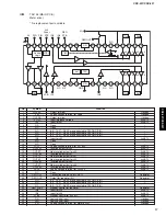
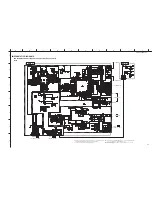
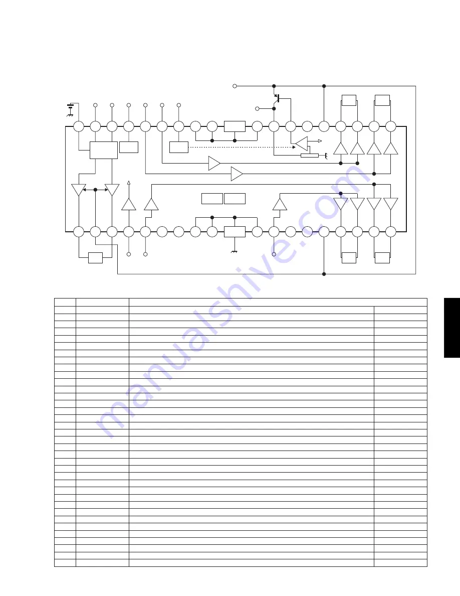
IC22
: TA2125 (MAIN P.C.B)
Motor driver
* No replacement part available.
36
35
34
33
32
31
30
29
28
FIN
RL4
RL3
RL2
RL5
RL1
27
26
25
24
23
22
21
20
19
1
2
3
4
5
6
7
8
9
FIN
TSD
lref
STBY
STBY
10
11
12
13
14
15
16
17
18
V
R
RIN
FIN
IN3
IN4
REG
STB
4ch
Driver
STB
N.C. N.C.
N.C.
N.C.
REG OUT
V
CC
IN2
GND
IN1
VCIN
+
+
+
N.C.
x 3
x 3
x 3
x 3
x 3
x 3
x 3
x 3
Control
Logic
No.
Symbol
Function
1
2
3
4
5
6
7
8
9
10
11
12
13
14
15
16
17
18
19
20
21
22
23
24
25
26
27
28
29
30
31
32
33
34
35
36
OUT5A
VM
OUT5B
VCIN
IN1
N.C.
N.C.
N.C.
N.C.
N.C.
IN2
N.C.
N.C.
VCC1
OUT2M
OUT2P
OUT1M
OUT1P
OUT3P
OUT3M
OUT4P
OUT4M
VCC2
N.C.
REG OUT
REG OUT
N.C.
N.C.
N.C.
REG STBY
IN4
IN3
STBY
FIN
RIN
VR
Output terminal
Supply voltage terminal for Logic
Output terminal
Input reference voltage
Input for ch1
Open
Open
8, 9, 10, 27, 28, 29 are connected to PW GND (FIN)
8, 9, 10, 27, 28, 29 are connected to PW GND (FIN)
8, 9, 10, 27, 28, 29 are connected to PW GND (FIN)
Input for ch2
Open
Open
Supply voltage terminal for ch 1/ch2
Inverted output for ch2
Non-inverted output for ch2
Inverted output for ch1
Non-inverted output for ch1
Non-inverted output for ch3
Inverted output for ch3
Non-inverted output for ch4
Inverted output for ch4
Supply voltage terminal for ch3/ch4
Open
Connection with BASE of PNP Tr
Output for regulator (5V)
8, 9, 10, 27, 28, 29 are connected to PW GND (FIN)
8, 9, 10, 27, 28, 29 are connected to PW GND (FIN)
8, 9, 10, 27, 28, 29 are connected to PW GND (FIN)
Standby control for regulator
Input for ch4
Input for ch3
Standby control for 4ch BTL
Logic control input
Logic control input
Supply voltage terminal for motor driver
H-bridge
H-bridge
H-bridge
4ch BTL
4ch BTL
–
–
–
–
–
4ch BTL
–
–
4ch BTL
4ch BTL
4ch BTL
4ch BTL
4ch BTL
4ch BTL
4ch BTL
4ch BTL
4ch BTL
4ch BTL
–
Regulator
Regulator
–
–
–
Regulator
4ch BTL
4ch BTL
4ch BTL
H-bridge
H-bridge
H-bridge
Содержание CDX-397
Страница 4: ...CDX 497 CDX 397 4 CDX 497 CDX 397 ...
Страница 27: ...CDX 497 CDX 397 27 MEMO MEMO MEMO MEMO ...


