AD824
41
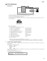
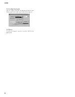
SLOT and CPU connection check
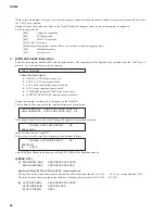
The first line on the screen shows the condition at the data bus from the left D15, D14. . . . D1, D0.
The second line on the screen shows the condition at the address bus from the left A15, A14 . . . A2, A1.
The third line on the screen shown the condition at other control lines from the left /CON-MY,/IRQ-MY, RX-MY, TX-MY.
For each item, an “0” is used to indicate normal and “X” is used to indicate an abnormality.
[3] SLOT CLOCK
XXX XXXX
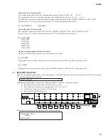
Connection check of slot clock line
The condition is shown from the left as 256FS-MY, 128FS-MY, 64FS-MY, SYNC-MY, FS-MY, WCLK-MY.
For each item, an “0” is used to indicate normal and “X” is used to indicate an abnormality.
[4] SLOT +20D
SLOT +5D
SLOT -5A
SLOT +5A
SLOT -15A
SLOT +15A
Slot power supply peripheral connection check
Only the NG systems from the test results will be shown on the screen.
[5] WC BNC
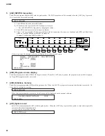
Displayed on the screen when the results of the word clock IN terminal/ JK901 and CPU connection are NG.
[6] COM B
Displayed on the screen when the results of the COM RS422 terminals/ CN903 and CPU connection are NG.
4.
[d01] LED inspection
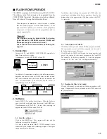
Select the test program number [d01] with the gain encoder. The LED inspection will be executed when the [+48V] key is pressed.
Or, it can also be executed by entering
When this program number is executed, the following sequence will occur. Check them visually.
1. The LEDs in the drawing below will come on one at a time.
2. The 7segLED will come on one column at time “0,1,2,3,4,5,6,7,8,8.”
3. All LEDs, except the level LEDs, will flash 3 times.
4. [d01] on the 7segLED will come on.
In addition, the following will be displayed on the terminal software.
AD824_DIAG>d01
+48V MASTER
PEAK
NOMINAL
SIGNAL
+48V
PEAK
NOMINAL
SIGNAL
+48V
GAIN
dB
44.1kHz 48kHz
BNC
SLOT
INTERNAL
WORD CLOCK
SEL
1
2
3
4
5
6
7
8
SEL
OFF
ON
POWER
DIAG[01]LED CHECK...............................................
............DONE
AD824_DIAG>
Содержание AD824
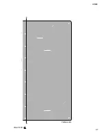
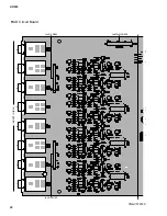
Страница 22: ...MAIN Circuit Board B B 3NA V579130 AD824 22 ...
Страница 23: ...E B B MAIN MYSL 3NA V579130 MYSL Circuit Board AD824 23 Pattern side Pattern side ...
Страница 24: ...3NA V579110 INPUT BAL 1 2 3 4 5 6 7 8 1 HA Circuit Board C C AD824 24 ...
Страница 25: ...AD824 25 3NA V579110 to MAIN CN903 1 C C to JK CN202 to JK CN102 to DC CN007 Component side ...
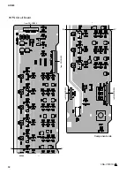
Страница 26: ...HA Circuit Board 3NA V579110 1 D D AD824 26 ...
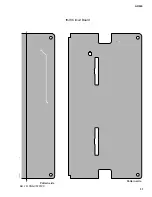
Страница 27: ...3NA V579110 1 D D AD824 27 Pattern side ...
Страница 28: ...AD824 28 3NA V579120 AD Circuit Board E E INSERT IN BAL to MAIN CN909 1 2 3 4 5 6 7 8 to JK CN203 to JK CN103 ...
Страница 30: ...AD824 30 AD Circuit Board 3NA V579120 F F ...
Страница 31: ...AD824 31 JK Circuit Board F F AD JK 3NA V579120 Pattern side Pattern side ...
Страница 33: ...PN Circuit Board 3NA V579100 1 H H H H AD824 33 Pattern side ...

