


22
www.xilinx.com
SP605 Hardware User Guide
UG526 (v1.1.1) February 1, 2010
Chapter 1:
SP605 Evaluation Board
References
See the System ACE CF product page for more information at
http://www.xilinx.com/support/documentation/system_ace_solutions.htm
.
In addition, see the
System ACE CompactFlash Solution Data Sheet
.
[Ref 5]
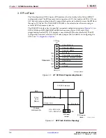
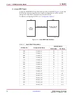
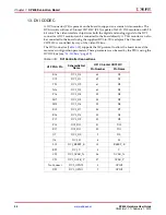
6. USB JTAG
JTAG configuration is provided through onboard USB-to-JTAG configuration logic where
a computer host accesses the SP605 JTAG chain through a Type-A (computer host side) to
Type-Mini-B (SP605 side) USB cable. The JTAG chain of the board is illustrated in
Figure 1-6
. JTAG configuration is allowable at any time under any mode pin setting. JTAG
initiated configuration takes priority over the mode pin settings.
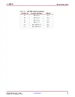
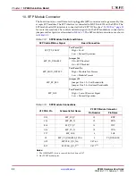
AA1
SYSACE_MPBRDY
39
MPBRDY
W4
SYSACE_MPCE
42
MPCE
AA2
SYSACE_MPIRQ
41
MPIRQ
T6
SYSACE_MPOE
77
MPOE
T5
SYSACE_MPWE
76
MPWE
G17
SYSACE_CFGTDI
81
CFGTDI
A21
FPGA_TCK
80
CFGTCK
E18
FPGA_TDI
82
CFGTDO
D20
FPGA_TMS
85
CFGTMS
N19
CLK_33MHZ_SYSACE(2)
93
CLK
Notes:
1. U17 System ACE CF controller 3.3V signals as named are wired to a set of TXB0108 3.3V-to-1.5V level
shifters. The nets between the 1.5V side of the level shifters and the U1 FPGA have the same names
with _LS appended.
2. The System ACE CF clock is sourced from U29 32.000MHz oscillator.
Table 1-8:
System ACE CF Connections
(Cont’d)
U1 FPGA Pin
Schematic Net Name
(1)
U17 XCCACETQ144I
Pin Number
Pin Name
X-Ref Target - Figure 1-6
Figure 1-6:
JTAG Chain Diagram
FMC LPC
TDO
U1
FPGA
TDI
T
S
TTDI
CFGTDO
CFGTDI
T
S
TTDO
TDO
S
y
s
tem ACE CF
3.3V
2.5V
TDI
B
u
ffer
U
S
B He
a
der
J4
J2
J19
U17
UG526_06_092409


