


74
ML40
x
EDK Processor Reference Design
UG082 (v5.0) June 30, 2006
Chapter 8:
PLB TFT LCD Controller
R
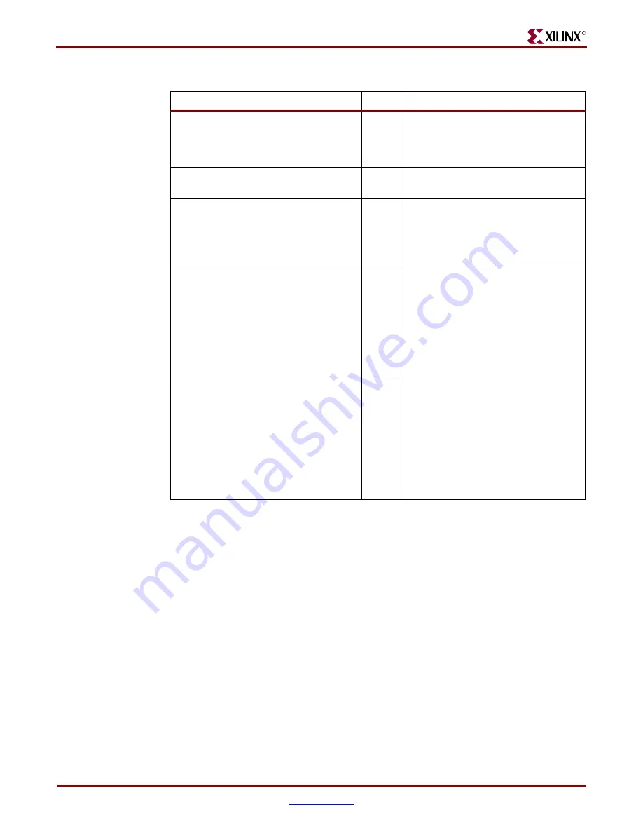
Table 8-5:
Parameters
Name
Default Description
C_DCR_BASEADDR
N/A
Base address of DCR control registers.
Must be aligned on an even DCR
address boundary (least significant bit
= 0).
C_DCR_HIGHADDR
N/A
Upper address boundary, must be set to
value of C_DCR_BA 1.
C_DEAFULT_TFT_BASE_ADDR[0:10]
N/A
Most significant bits of base address for
video memory. The 11 most significant
bits of this address define the 2 MB
region of memory used for the video
frame storage.
C_DPS_INIT
1
Initial reset state of DPS control bit:
0 = DPS output bit resets to 0.
This initializes the display to use a
normal scan direction.
1 = DPS output bit resets to 1.
This initializes the display to use a
reverse scan direction (rotates screen
180 degrees).
C_ON_INIT
1
Initial reset state of TFT enable/disable
bit:
0 = Disable TFT display on reset.
This causes a black screen to be
displayed on reset.
1 = Enable TFT display on reset.
This causes the PLB TFT LCD
controller to operate normally on
reset.
Содержание ML40 Series
Страница 1: ...R ML40x EDK Processor Reference Design User Guide for EDK 8 1 UG082 v5 0 June 30 2006...
Страница 6: ...6 www xilinx com ML40x EDK Processor Reference Design UG082 v5 0 June 30 2006 R...
Страница 8: ...8 www xilinx com ML40x EDK Processor Reference Design UG082 v5 0 June 30 2006 R...
Страница 14: ...14 www xilinx com ML40x EDK Processor Reference Design UG082 v5 0 June 30 2006 Preface About This Guide R...