


62
ML40
x
EDK Processor Reference Design
UG082 (v5.0) June 30, 2006
Chapter 7:
OPB PS/2 Controller (Dual)
R
Module Port Interface
Information about the signals, pins, and parameters for the module is listed in tables
, and
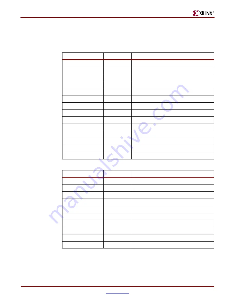
Table 7-1:
OPB Slave Signals
Name
Direction
Description
IPIF_Rst
Input
OPB system reset
OPB_BE[0:3]
Input
OPB byte enables
OPB_Select Input
OPB
select
OPB_Dbus[0:31]
Input
OPB data bus
OPB_Clk
Input
OPB system clock
OPB_Abus[0:31]
Input
OPB address bus
OPB_RNW
Input
OPB read not write
OPB_seqAddr
Input
OPB sequential address
Sln_XferAck
Output
Slave transfer acknowledge
Sln_Dbus[0:31]
Output
Slave data bus
Sln_DBusEn
Output
Slave data bus enable
Sln_errAck
Output
Slave error acknowledge
Sln_retry
Output
Slave bus cycle retry
Sln_toutSup
Output
Slave timeout suppress
Table 7-2:
External I/O Pins
Name
Direction
Description
Sys_Intr1
Output
Interrupt, Port #1
Clkin1
Input
PS/2 Clock In, Port #1
Clkpd1
Output
PS/2 Clock Pulldown, Port #1
Rx1
Input
PS/2 Serial Data In, Port #1
Txpd1
Output
PS/2 Serial Data Out Pulldown, Port #1
Sys_Intr2 Output
Interrupt,
Port
#2
Clkin2
Input
PS/2 Clock In, Port #2
Clkpd2
Output
PS/2 Clock Pulldown, Port #2
Rx2
Input
PS/2 Serial Data In, Port #2
Txpd2
Output
PS/2 Serial Data Out Pulldown, Port #2
Содержание ML40 Series
Страница 1: ...R ML40x EDK Processor Reference Design User Guide for EDK 8 1 UG082 v5 0 June 30 2006...
Страница 6: ...6 www xilinx com ML40x EDK Processor Reference Design UG082 v5 0 June 30 2006 R...
Страница 8: ...8 www xilinx com ML40x EDK Processor Reference Design UG082 v5 0 June 30 2006 R...
Страница 14: ...14 www xilinx com ML40x EDK Processor Reference Design UG082 v5 0 June 30 2006 Preface About This Guide R...