23
Set Parameters of Serial Port 1 (COM C).
Serial Port 2 Configuration
Set Parameters of Serial Port 2 (COM D).
Serial Port 3 Configuration
Set Parameters of Serial Port 3 (COM E).
Serial Port 4 Configuration
Set Parameters of Serial Port 4 (COM F).
Serial Port Console Redirection
Serial Port Console Redirection.
Chipset
Host Bridge/South Bridge
This screen provides information on Host Bridge/South Bridge parameters.
Содержание WLP-7A20 Series
Страница 7: ...VII Version Change History Date Version Description Remark 2014 9 24 V1 0 First release Ivy...
Страница 9: ...IX...
Страница 15: ...5 System View WTP 9A66 Outline Drawing...
Страница 16: ...6 WTP 9A66 Outline Drawing...
Страница 17: ...7 I O connectors Note Share the same place with DVI output DVI and VGA not simultaneously...
Страница 19: ...9...
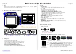
Страница 21: ...11 Getting Started This chapter tells you how to set up the system...
Страница 39: ...29 JP5 Backlight Adjust Description Jumper Setting analog Inverter 1 2 default PWM Inverter 2 3...
Страница 41: ...31 JP7 Touch Panel Type Selection Description Jumper Setting 3M type 1 2 3 4 default ELO type 5 6 7 8...
Страница 43: ...33 JP9 TPM Settings Description Jumper Setting Clear ME RTC registers 1 2 Keep ME RTC registers OPEN default...
Страница 44: ...34 JP10 CMOS Clear Description Jumper Setting Normal Open 1 2 default CMOS Clear 2 3...
Страница 45: ...35 JP11 Thermal sensor Description Jumper Setting Auto detect 1 2 default always 25 2 3 always 40 NC...
Страница 46: ...36 JP12 SATA or SATA DOM Selection Description Jumper Setting SATA DOM 1 2 power 5V SATA 2 3 default GND...
Страница 48: ...38 Connector Definition...
Страница 49: ...39 PJ5 HDD Power Connector Pin Signal Description 1 12V 2 Ground 3 Ground 4 5V...
Страница 50: ...40 PJ6 HDD Power Connector Pin Signal Description 1 12V 2 Ground 3 Ground 4 5V...
Страница 52: ...42 PJ8 Power Jack Connector Pin Signal Description 1 DC In 2 DC In 3 Ground 4 Ground 1 5 5 Ground...
Страница 53: ...43 J5 J6 J7 Internal USB 3 3V Interface Pin Signal Description 1 3 3VS 2 Data 3 Data 4 Ground 5 Ground...
Страница 57: ...47 J13 F W IC EETI control Pin Signal Description 1 3 3V_TP 2 C2CK 3 C2D 4 Ground...
Страница 58: ...48 J14 J15 Internal USB 5V Interface Pin Signal Description 1 5VSB 2 5VSB 3 Data 4 Data 5 Ground 6 Ground...
Страница 61: ...51 J19 Battery Socket Pin Signal Description 1 RTC 3 3V 2 GND...
Страница 68: ...58 J26 SDP EC Simple Debug Port Pin Signal Description 1 5V 2 P80_DAT 3 P80_CLK 4 Ground...
Страница 73: ...63 J31 Light Sensor Connector For Outdoor Pin Signal Description 1 Light Sensor 2 NC 3 3 3V...
Страница 74: ...64 J32 EC Reset Pin Signal Description 1 VCC_POR 2 GND...
Страница 75: ...65 J33 HEATER CLEAR ME LED INDICATE Pin Signal Description 1 3 3V_UC 2 HEATER_LED 3 KEYLOCK_LED...
Страница 76: ...66 J34 J36 Standard SATA Interface Pin Signal Description 1 Ground 2 Tx 3 Tx 4 Ground 5 Rx 6 Rx 7 Ground...
Страница 80: ...70 J41 POWER HDD LED For WMP 176 196 Pin Signal Description 1 SATA LED 2 3 3V 3 3 3V 4 Power LED...
Страница 81: ...71 J42 ATX 12V Connect For Heater Power Pin Signal Description 1 12V 2 12V 3 Ground 4 Ground...
Страница 83: ...73 J44 Handset Connect Pin Signal Description 1 HOOK_ON 2 Handset speaker 3 Handset MIC 4 GND...
Страница 84: ...74 J47 Power Switch connect Pin Signal Description 1 Power ON 2 GND...
Страница 85: ...75 J48 J49 Ethernet Port Pin Signal Description 1 Data0 2 Data0 3 Data1 4 Data2 5 Data2 6 Data1 7 Data3 8 Data3...
Страница 86: ...76 J50 J51 USB1 2 3 4 Port Pin Signal Description 1 5V 2 Data 3 Data 4 GND...
Страница 88: ...78 J53 J54 Audio Connector Pin Signal Description J53 Microphone stereo Pink J54 Line Out stereo Green...
Страница 89: ...79 J55 Reset connector Pin Signal Description 1 SYS_RESET 2 GND...
Страница 90: ...80 J56 Reset Button Pin Signal Description 1 SYS_RESET 2 GND...