CONFIDENTIAL – DO NOT COPY
Page 7-34
File No. SG-0211
The DQ and DQS outputs are in the High-Z state, where they remain until driven in
normal operation (by a read access). After all power supply and reference voltages are
stable, and the clock is stable, the DDR SDRAM requires a 200µs delay prior to
applying an executable command.
Once the 200µs delay has been satisfied, a Deselect or NOP command should be
applied, and CKE must be brought HIGH. Following the NOP command, a Precharge
ALL command must be applied. Next a Mode Register Set command must be issued
for the Extended Mode Register, to enable the DLL, then a Mode Register Set
command must be issued for the Mode Register, to reset the DLL, and to program the
operating parameters. 200 clock cycles are required between the DLL reset and any
read command. A Precharge ALL command should be applied, placing the device in
the “all banks idle” state Once in the idle state, two auto refresh cycles must be
performed. Additionally, a Mode Register Set command for the Mode Register, with the
reset DLL bit deactivated (i.e. to program operating parameters without resetting the
DLL) must be performed.
Following these cycles, the DDR SDRAM is ready for normal operation.
DDR SDRAM’s may be reinitialized at any time during normal operation by asserting a
valid MRS command to either the base or extended mode registers without affecting
the contents of the memory array. The contents of either the mode register or extended
mode register can be modified at any valid time during device operation without
affecting the state of the internal address refresh counters used for device refresh.
Содержание VW42L HDTV10A
Страница 42: ...CONFIDENTIAL DO NOT COPY Page 7 11 File No SG 0211 PIN ASSIGNMENT ...
Страница 43: ...CONFIDENTIAL DO NOT COPY Page 7 12 File No SG 0211 PIN DESCRIPTION ...
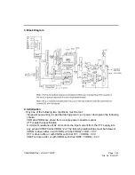
Страница 52: ...CONFIDENTIAL DO NOT COPY Page 7 21 File No SG 0211 BLOCK DIAGRAM ...
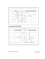
Страница 59: ...CONFIDENTIAL DO NOT COPY Page 7 28 File No SG 0211 Fig D READ TIMING WAVEFORMS ...
Страница 60: ...CONFIDENTIAL DO NOT COPY Page 7 29 File No SG 0211 Fig E RESET TIMING WAVEFORM ...
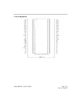
Страница 62: ...CONFIDENTIAL DO NOT COPY Page 7 31 File No SG 0211 1 Pin Configuration ...
Страница 63: ...CONFIDENTIAL DO NOT COPY Page 7 32 File No SG 0211 2 Input Output Functional Description ...
Страница 66: ...CONFIDENTIAL DO NOT COPY Page 7 35 File No SG 0211 5 Register Definition ...
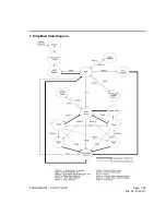
Страница 69: ...CONFIDENTIAL DO NOT COPY Page 7 38 File No SG 0211 7 Simplified State Diagram ...
Страница 70: ...CONFIDENTIAL DO NOT COPY Page 7 39 File No SG 0211 8 Absolute Maximum Ratings 9 Capacitance ...
Страница 74: ...CONFIDENTIAL DO NOT COPY Page 7 43 File No SG 0211 Block Diagram ...
Страница 75: ...CONFIDENTIAL DO NOT COPY Page 7 44 File No SG 0211 Pin Description Pin Description Maximum Ratings ...
Страница 81: ...CONFIDENTIAL DO NOT COPY Page 8 5 File No SG 0211 CH1 DACBCLK U28 PIN4 CH1 DACMCLK U28 PIN5 ...
Страница 95: ...CONFIDENTIAL DO NOT COPY Page 10 3 File No SG 0211 Main Board Block Diagram ...
Страница 96: ......
Страница 97: ......
Страница 98: ......


