CONFIDENTIAL – DO NOT COPY
Page 7-26
File No. SG-0211
RESET OPERATION
01The RESET pin provides a hardware method of resetting the device to reading array
data. When the RESET pin is driven low for at least a period of tRP, the device
immediately terminates any operation in progress, tristates all output pins, and ignores
all read/write commands for the duration of the RESET pulse. The device also resets
the internal state machine to reading array data. The operation that was interrupted
should be reinitiated once the device is ready to accept another command sequence,
to ensure data integrity.
Current is reduced for the duration of the RESET pulse. When RESET is held at
VSS 0.3V, the device draws CMOS standby current (ICC4). If RESET is held at VIL
but not within VSS 0.3V, the standby current will be greate
r.The RESET pin may be
tied to system reset circuitry. A system reset would that also reset the Flash memory,
enabling the system to read the boot-up firm-ware from the Flash memory.
If RESET is asserted during a program or erase operation, the RY/BY pin remains a "0"
(busy) until the internal reset operation is complete, which requires a time of tREADY
(during Embedded Algorithms). The system can thus monitor RY/BY to determine
whether the reset operation is complete. If RESET is asserted when a program or
erase operation is not executing (RY/BY pin is "1"), the reset operation is completed
within a time of tREADY (not during Embedded Algorithms). The system can read data
tRH after the RESET pin returns to VIH. Refer to the AC Characteristics tables for
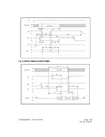
RESET parameters and to Figure 14 for the timing diagram.
WRITE PROTECT (WP)
The write protect function provides a hardware method to protect boot sectors without
using VID.
If the system asserts VIL on the WP/ACC pin, the device disables program and erase
functions in the two "outermost" 8 Kbyte boot sectors independently of whether those
sectors were protected or unprotected using the method described in Sector/Sector
Group Protection and Chip Unprotection". The two outermost 8 Kbyte boot sectors are
the two sectors containing the lowest addresses in a bottom-boot-configured device, or
the two sectors containing the highest addresses in a top-boot-configured device.
If the system asserts VIH on the WP/ACC pin, the device reverts to whether the two
outermost 8K Byte boot sectors were last set to be protected or unprotected. That is,
sector protection or unprotection for these two sectors depends on whether they were
last protected or unprotected using the method described in "Sector/Sector Group
Protection and Chip Unprotection".
Note that the WP/ACC pin must not be left floating or unconnected; inconsistent
behavior of the device may result.
Содержание VW42L HDTV10A
Страница 42: ...CONFIDENTIAL DO NOT COPY Page 7 11 File No SG 0211 PIN ASSIGNMENT ...
Страница 43: ...CONFIDENTIAL DO NOT COPY Page 7 12 File No SG 0211 PIN DESCRIPTION ...
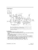
Страница 52: ...CONFIDENTIAL DO NOT COPY Page 7 21 File No SG 0211 BLOCK DIAGRAM ...
Страница 59: ...CONFIDENTIAL DO NOT COPY Page 7 28 File No SG 0211 Fig D READ TIMING WAVEFORMS ...
Страница 60: ...CONFIDENTIAL DO NOT COPY Page 7 29 File No SG 0211 Fig E RESET TIMING WAVEFORM ...
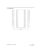
Страница 62: ...CONFIDENTIAL DO NOT COPY Page 7 31 File No SG 0211 1 Pin Configuration ...
Страница 63: ...CONFIDENTIAL DO NOT COPY Page 7 32 File No SG 0211 2 Input Output Functional Description ...
Страница 66: ...CONFIDENTIAL DO NOT COPY Page 7 35 File No SG 0211 5 Register Definition ...
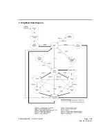
Страница 69: ...CONFIDENTIAL DO NOT COPY Page 7 38 File No SG 0211 7 Simplified State Diagram ...
Страница 70: ...CONFIDENTIAL DO NOT COPY Page 7 39 File No SG 0211 8 Absolute Maximum Ratings 9 Capacitance ...
Страница 74: ...CONFIDENTIAL DO NOT COPY Page 7 43 File No SG 0211 Block Diagram ...
Страница 75: ...CONFIDENTIAL DO NOT COPY Page 7 44 File No SG 0211 Pin Description Pin Description Maximum Ratings ...
Страница 81: ...CONFIDENTIAL DO NOT COPY Page 8 5 File No SG 0211 CH1 DACBCLK U28 PIN4 CH1 DACMCLK U28 PIN5 ...
Страница 95: ...CONFIDENTIAL DO NOT COPY Page 10 3 File No SG 0211 Main Board Block Diagram ...
Страница 96: ......
Страница 97: ......
Страница 98: ......


