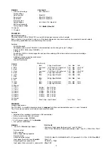
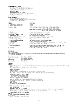


TDA9875:
General description:
The TDA9875 is a single-chip Digital TV Sound Processor (DTVSP) for analogue and digital multi-channel sound systems.
Features:
Demodulator and decoder section:
• Sound IF (SIF) input switch e.g. to select between terrestrial TV SIF and SAT SIF sources
• SIF AGC with 21 dB control range
• SIF 8-bit Analogue-to-Digital Converter (ADC)
• DQPSK demodulation for different standards, simultaneously with 1-channel FM demodulation
• NICAM decoding (B/G, I and L standard)
• Two-carrier multistandard FM demodulation (B/G, D/K and M standard)
• Decoding for three analogue multi-channel systems (A2, A2+ and A2*) and satellite sound
• Optional AM demodulation for system L, simultaneously with NICAM
• Programmable identification (B/G, D/K and M standard) and different identification times
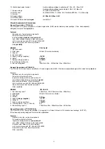
DSP section:
• Digital crossbar switch for all digital signal sources and destinations
• Control of volume, balance, contour, bass, treble, pseudo stereo, spatial, bass boost and soft-mute
• Plop-free volume control
• Automatic Volume Level (AVL) control
• Adaptive de-emphasis for satellite
• Programmable beeper
• Monitor selection for FM/AM DC values and signals, with peak detection option
• PS-bus interface for a feature extension (e.g. Dolby surround) with matrix, level adjust and mute.
Analogue audio section:
• Analogue crossbar switch with inputs for mono and stereo, SCART 1 input/output, SCART2 input/output and line output
• User defined full-level/-3dB scaling for SCART outputs
• Output selection of mono, stereo, dual A/B, dual A or dual B
• 20 kHz bandwith for SCART-to-SCART copies
• Standby mode with functionality for SCART copies
• Dual audio digital-to-analogue converter from DSP to analogue crossbar switch, bandwith 15kHz
• Dual audio ADC from analogue inputs to DSP
• Two dual audio Digital-to-Analogue Converters (DACs) for loudspeakers (Main) and headphone (Auxiliary) outputs;
also applicable for L, R, C and S in the Dolby Pro Logic mode with feature extension.
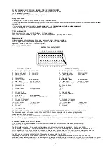
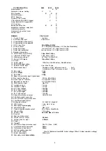
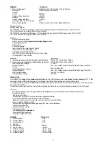
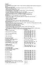
PINNING
1. NICAM clock output (728kHz)
2. Serial NICAM DATA output (728kHz)
3. First PC-bus slave address modifier
4. SCL (PC-bus clock)
5. SDA (PC-bus data)
6. Analogue supply ground 1
7. Analogue supply voltage 1
8. Resistor for reference current generator
9. First general purpose I/O pin
10. Sound IF input 2
1 1 . Reference voltage for demodulator part
12. Sound IF input 1
13. Second PC-bus slave address modifier
14. Digital supply ground 1
15. Digital supply voltage 1
16. Capacitor for power-on reset
17. Crystal oscillator output
18. Crystal oscillator input
19. Tuning voltage output for crystal oscillator
20. Second general purpose I/O pin
21. System clock output
22. PS-bus clock
23. PS-bus word select
24. PS-bus data output 2
25. PS-bus data output 1
26. PS-bus data input 2
27. PS-bus data input 1
28. First test pin; connected to ground for normal operation
29. Audio mono input
30.Second test pin; connected to ground tor normal operation
31. External audio input right channel
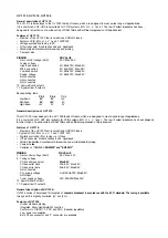
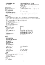
PIN VALUE
LOW level input voltage Max 0.8V
HIGH level input voltage Min 2.0V
LOW level input voltage Max 0.8V
HIGH level input voltage Min 2.0V
LOW level input voltage Max 0.8V
HIGH level input voltage Min 2.0V
LOW level input voltage Max 1.6V
HIGH level input voltage Min 3.0V
LOW level input voltage Max 0.8V
HIGH level input voltage Min 2.0V
0V
5V, Min : 4.75V, Max : 5.5V
Iref: 220mA, Min : 170mA, Max : 260mA
Min : 21Vrms, Max : 250mVrms
Vdda1/Vssa1 : 50%, Min : 35%, Max : 65%
Min : 21Vrms, Max : 250mVrms
LOW level input voltage : Max : 0.8V
HIGH level input voltage : Min : 2.0V
0V
5V, Min : 4.75V, Max : 5.5V
LOW level input voltage : Max : 1.6V
HIGH level input voltage : Min : 3.0V
LOW level input voltage
HIGH level input voltage
LOW level input voltage
HIGH level input voltage
LOW level input voltage
HIGH level input voltage
LOW level input voltage
HIGH level input voltage
LOW level input voltage
HIGH level input voltage
LOW level input voltage
HIGH level input voltage
LOW level input voltage
HIGH level input voltage
500mVrms
350mVrms
Max
Min
Max
Min
Max
Min
Max
Min
Max
Min
Max
Min
Max
Min
0.5V
2.9V
0.8V
2.0V
0.8V
2.0V
0.8V
2.0V
0.8V
2.0V
0.8V
2.0V
0.8V
2.0V
16
Содержание 11AK19
Страница 1: ...SERVICE MANUAL CHASSIS 11 AK19 FIRMEN EUROLINE PALLADIUM S E G TECHLINE VESTEL...
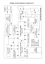
Страница 27: ...GENERAL BLOCK DIAGRAM OF CHASSIS AK19 26...
Страница 30: ......
Страница 31: ......
Страница 32: ......
Страница 33: ......
Страница 34: ......
Страница 35: ......
Страница 36: ......
Страница 37: ......
Страница 38: ......
Страница 39: ......
Страница 40: ...SERVICE MANUAL VESTEL 11AK19 MODEL...