background image

Physical Details 

EBX-11 Reference Manual 

15


H

ARDWARE 

A

SSEMBLY


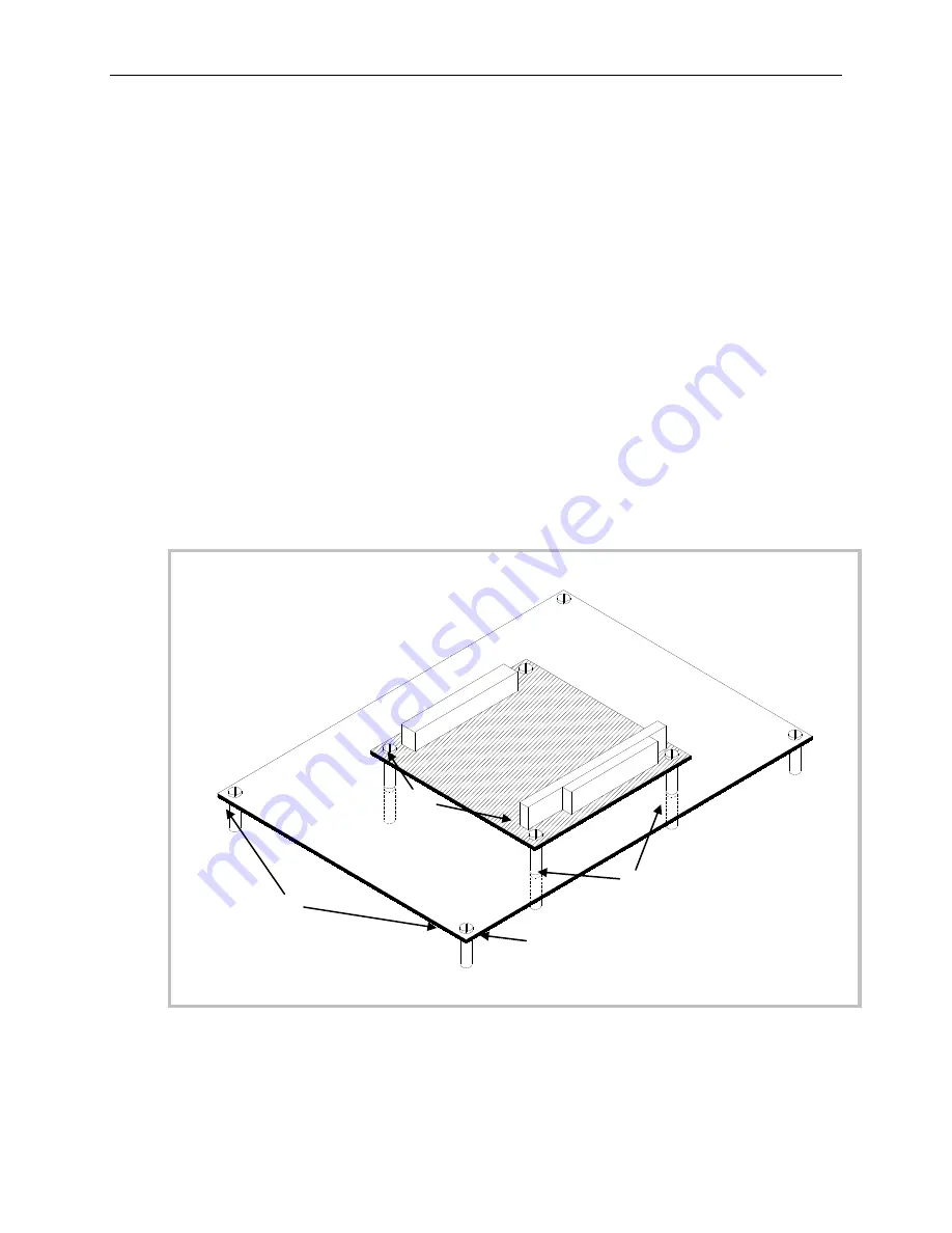
The EBX-11 mounts on four hardware standoffs using the corner mounting holes (A). These 
standoffs are secured to the underside of the circuit board using pan head screws. 

Four additional standoffs (B) must be used under the circuit board to prevent excessive flexing 
when expansion modules are mated and separated. These are secured with four male-female 
standoffs (C), threaded from the top side, which also serve as mounting struts for the PC/104 
stack. 

The entire assembly can sit on a table top or be secured to a base plate. When bolting the unit 
down, make sure to secure all eight standoffs (A and B) to the mounting surface to prevent 
circuit board flexing. 

An extractor tool is available (part number VL-HDW-201) to separate the PC/104 modules from 
the stack. 

Note 

Standoffs and screws are available as part number VL-HDW-101. 

S

TANDOFF 

L

OCATIONS


Figure 8. Standoff Locations 


C


B


A


Connect this mounting hole to earth to make 
TVS devices functional. See Transient Voltage 
Suppression (TVS) Devices.
 

StockCheck.com

Содержание Python EBX-11

Страница 1: ...Reference Manual DOC REV 9 18 2014 EBX 11 Python AMD LX 800 Based SBC with Ethernet Video Audio Industrial I O and SPI S t o c k C h e c k c o m...

Страница 2: ...is error free VersaLogic makes no representations or warranties with respect to this product and specifically disclaims any implied warranties of merchantability or fitness for any particular purpose...

Страница 3: ...contained a nonstandard Digital I O signaling on the J5 connector See J5 I O Connector on page 27 for details The pinout will be corrected with the Rev 5 release Rev 3 Release Pre production only No c...

Страница 4: ...CMOS Setup 10 Operating System Installation 11 Physical Details 12 Dimensions and Mounting 12 Hardware Assembly 15 Standoff Locations 15 External Connectors 16 EBX 11 Connectors 16 EBX 11 Connector Fu...

Страница 5: ...rating System on CompactFlash 37 Programmable LED 38 External Speaker 38 Push Button Reset 38 Video Interface 39 Configuration 39 Video BIOS Selection 39 SVGA Output Connector 39 LVDS Flat Panel Displ...

Страница 6: ...d Tachometer Inputs 56 External Connections 56 PWM Output and TACH Input Code Example 56 PC 104 Expansion Bus 59 PC 104 I O Support 59 PC 104 Memory Support 59 IRQ Support 59 DMA Support 59 System Res...

Страница 7: ...timer Vcc sensing reset circuit all rails monitored interrupt on fault EBX compliant 5 75 x 8 00 footprint Field upgradeable BIOS with OEM enhancements Latching I O connectors Customizing available Th...

Страница 8: ...51ER based Fast Ethernet 10 100 Controllers Audio Interface AC 97 compatible Line Out and Line In support Analog Input 8 channel 12 bit single ended 500 kSPS channel independent input range 0 to 4 095...

Страница 9: ...Introduction EBX 11 Reference Manual 3 EBX 11 Block Diagram RS 232 422 2 Ports to J5 S t o c k C h e c k c o m...

Страница 10: ...y wearing a grounded antistatic wrist strap Keep all plastic away from the board and do not slide the board over any surface After removing the board from its protective wrapper place the board on a g...

Страница 11: ...board s lower right mounting hole as shown in Figure 2 All other mounting holes are floating Use metal standoffs or a grounding strap to connect the lower right mounting hole to the enclosure chassis...

Страница 12: ...lease provide the following information Your name the name of your company your phone number and e mail address The name of a technician or engineer that can be contacted if any questions arise Quanti...

Страница 13: ...ble CBR 2022 You will also need a Windows or other OS installation CD Basic Setup The following steps outline the procedure for setting up a typical development system The EBX 11 should be handled at...

Страница 14: ...Attach the motherboard connector of the ATX power supply to the adapter 3 Attach Cables and Peripherals Plug the video adapter cable CBR 1201 into socket J6 Attach the video monitor interface cable to...

Страница 15: ...to the EBX 11 and peripheral devices 5 Power On Turn on the ATX power supply and the video monitor If the system is correctly configured a video signal should be present 6 Change CMOS Setup Settings E...

Страница 16: ...LOPPY DRIVE TYPES Ide 1 3 AUTOCONFIG LBA 631KB Floppy 0 Not installed Ide 2 3 AUTOCONFIG LBA Ext Floppy 1 Not installed Ide 3 3 AUTOCONFIG LBA 219MB Features Configuration System BIOS Setup Advanced C...

Страница 17: ...itecture used on the EBX 11 makes the installation and use of most of the standard x86 processor based operating systems very simple The operating systems listed on the VersaLogic OS Compatibility Cha...

Страница 18: ...EBX standards which provide for specific mounting hole and PC 104 Plus stack locations as shown in the diagram below Figure 4 EBX 11 Dimensions and Mounting Holes 3 0 20 0 00 0 20 1 875 0 00 5 80 2 65...

Страница 19: ...lexing when expansion modules are mated and demated Flex damage caused by excessive force on an improperly mounted circuit board is not covered under the product warranty Figure 5 EBX 11 Height Dimens...

Страница 20: ...Physical Details EBX 11 Reference Manual 14 Figure 7 CBR 4004 Dimensions and Mounting Holes J1 J2 J3 J4 J6 J7 J8 J9 J5 2 37 2 87 0 25 0 25 0 40 1 95 0 70 0 63 0 62 0 06 S t o c k C h e c k c o m...

Страница 21: ...m the top side which also serve as mounting struts for the PC 104 stack The entire assembly can sit on a table top or be secured to a base plate When bolting the unit down make sure to secure all eigh...

Страница 22: ...y J6 SVGA J9 LVDS J21 USB 3 V3 V2 V1 J16 Factory Use Only J17 SPI J12 IDE J5 Analog PWM Digital I O J10 Audio Digital I O USB 0 1 J18 LPT Pin 1 J4 COM 1 4 PLED PS 2 Keyboard and Mouse Reset Button Spe...

Страница 23: ...700 0 060 39 J7 PC 104 Plus AMP 1375799 1 2 106 3 096 J9 LVDS 20 pin PanelMate 1 25mm CBR 2010 or CBR 2011 18 bit TFT FPD using 20 pin Hirose 18 bit TFT FPD using 20 pin JAE 2 400 0 190 40 J10 Audio D...

Страница 24: ...COM2 Kycon K42 E9P P A4N Dual stacked DB 9 male J4 PS 2 Keyboard and Mouse Kycon KMDG 6S 6S S4N Dual stacked PS 2 female J5 COM4 Conta Clip 10250 4 5 pin screw terminal J6 COM3 Conta Clip 10250 4 5 pi...

Страница 25: ...Figure 11 CBR 4004 Connectors CBR 4004 connector functions depend on the I O connector to which it is attached J5 or J10 See Table 5 J5 or Table 7 J10 for details 2 1 40 39 J1 J2 J3 J4 J6 J7 J8 J9 5 1...

Страница 26: ...cal Details EBX 11 Reference Manual 20 Jumper Blocks JUMPERS AS SHIPPED CONFIGURATION Figure 12 Jumper Block Locations CPU Battery V3 V2 V1 1 3 2 4 1 3 5 7 2 4 6 8 1 2 3 V1 V2 V3 S t o c k C h e c k c...

Страница 27: ...Purpose Input In CPU reads bit as 1 Out CPU reads bit as 0 In 63 V2 5 6 Video BIOS Selector In Primary Video BIOS selected Out Secondary Video BIOS selected The secondary video BIOS is field upgradea...

Страница 28: ...Power Input 10 GND Ground Pin 1 is typically used in EPIC style power cables as a PS ON signal Since the EBX 11 does not support soft off pin 1 is internally connected to ground Pin 6 is typically us...

Страница 29: ...y under normal use is approximately 10 years CPU The Geode LX 800 microcontroller has a 32 bit low voltage AMD x86 microprocessor at its core The maximum clock rate is 500 MHz actual with 800 MHz Cele...

Страница 30: ...e system whenever the main CMOS RAM values are blank or when the system battery is dead or has been removed from the board SAVING CMOS SETUP PARAMETERS AS CUSTOM DEFAULTS To save CMOS Setup parameters...

Страница 31: ...time clock calendar chip Under normal battery conditions the clock maintains accurate timekeeping functions when the board is powered off SETTING THE CLOCK The CMOS Setup utility accessed by pressing...

Страница 32: ...009B Connector Pin Signal 1 COM1 1 Data Carrier Detect COM4 RS 232 RS 422 2 J3 6 Data Set Ready 26 J5 1 Ground 485 GND Ground 3 Top DB9 2 Receive Data 27 5 RTS TxD 4 7 Request to Send 28 4 TXD TxD 5 3...

Страница 33: ...8 PWM_OUT3 3 IO7 9 NC 2 IO8 10 GND 1 GND1 11 Digital I O 0 J3 5 IO9 12 Digital I O 1 Digital IO 4 IO10 13 Digital I O 2 3 IO11 14 Digital I O 3 2 IO12 15 GND 1 GND2 16 Digital I O 4 J4 5 IO13 17 Digit...

Страница 34: ...I O 2 17 Digital IO 4 IO14 18 Digital I O 6 18 3 IO15 19 Digital I O 5 19 2 IO16 20 GND 20 1 GND2 21 Digital I O 7 21 J6 1 IO17 22 Digital I O 9 22 Digital IO 2 IO18 23 Digital I O 8 23 3 IO19 24 Dig...

Страница 35: ...I O 18 3 IO11 14 Digital I O 19 2 IO12 15 GND 1 GND2 16 Digital I O 20 J4 5 IO13 17 Digital I O 21 Digital IO 4 IO14 18 Digital I O 22 3 IO15 19 Digital I O 23 2 IO16 20 GND 1 GND2 21 Digital I O 24 J...

Страница 36: ...te 2 Ground Ground 24 Ground Ground 3 DD7 Data bus bit 7 25 DIOR I O read 4 DD8 Data bus bit 8 26 Ground Ground 5 DD6 Data bus bit 6 27 IORDY I O ready 6 DD9 Data bus bit 9 28 Ground Ground 7 DD5 Data...

Страница 37: ...f up to 460k baud IRQ lines are chosen in the CMOS Setup Each COM port can be independently enabled or disabled in CMOS Setup COM PORT CONFIGURATION There are no configuration jumpers for COM1 and COM...

Страница 38: ...RS 232 1 10 DCD 2 11 RXD 3 12 TXD 4 13 DTR 5 14 Ground 6 15 DSR 7 16 RTS 8 17 CTS 9 18 RI Note On Rev 4 boards the COM3 and COM4 connectors have a nonstandard pinout The RxD and RxD signals are transp...

Страница 39: ...tup screen This connector uses IEC 61000 4 2 rated TVS components to help protect against ESD damage Table 12 LPT Parallel Port Pinout J18 Pin Centronics Signal Signal Direction 1 Strobe Out 2 Auto fe...

Страница 40: ...board and mouse is protected by a 1 Amp fuse This connector uses IEC 61000 4 2 rated TVS components to help protect against ESD damage Table 13 PS 2 Mouse and Keyboard CBR 5009 J4 Top Pin Signal Descr...

Страница 41: ...isabled in CMOS Setup The USB controller uses PCI interrupt INTD CMOS Setup is used to select the IRQ line routed to each PCI interrupt line Table 14 USB Interface Connector J10 CBR 4004 J1 Pin Signal...

Страница 42: ...nnector J13 Rev 4 01 and Earlier J13 Pin Signal Name Function 1 USBP2PWR 5V Protected 3 USBP2 Channel 2 Data 5 USBP2 Channel 2 Data 7 GND Ground 9 GND Ground 2 USBP3PWR 5V Protected 4 USBP3 Channel 3...

Страница 43: ...Systems 512 MB SSD C51MI 3012 Silicon Systems 512 MB SSD C51M 3500 Silicon Systems 512 MB SSD C51MI 3500 Silicon Systems 1 GB SSD C01G 3012 Silicon Systems 1 GB SSD C01G 3500 Silicon Systems 2 GB SSD...

Страница 44: ...bit D7 in I O port 1D0h or 1E0h When changing the register make sure not to alter the value of the other bits The following code examples show how to turn the LED on and off Refer to page 59 for furt...

Страница 45: ...ST VIDEO BIOS SELECTION Jumper V2 5 6 can be removed to allow the system to boot off of the Secondary Video BIOS Unlike the Primary Video BIOS the Secondary Video BIOS can be reprogrammed in the field...

Страница 46: ...ting to use contact Support VersaLogic com for a custom video BIOS The 3 3V power provided to pins 19 and 20 of J9 is protected by a 1 Amp fuse See the connector location diagram on page 16 for pin an...

Страница 47: ...raction In the Features Configuration screen there is an option to control console redirection This option can be set to Auto or Redirect When set to Auto the console will not be redirected to COM1 un...

Страница 48: ...OFF Active cable not plugged in or cable not plugged into active hub Yellow LED Activity ON Activity detected on cable OFF No Activity detected on cable ETHERNET CONNECTOR Board mounted RJ 45 connecto...

Страница 49: ...up screen is used to select the IRQ line routed to INTB The audio controller can be disabled within the CMOS setup Table 21 Audio Connector CBR 4004 J10 Pin Signal Name Function 37 AUDINR Line In Righ...

Страница 50: ...r and any number of data frames can be sent The user must command the slave select high to complete the transaction The SPI clock rate can be software configured to operate at speeds between 1 MHz and...

Страница 51: ...h 0 0 8 bit 0 1 16 bit 1 0 24 bit 1 1 32 bit D3 MAN_SS SPI Manual Slave Select Mode This bit determines whether the slave select lines are controlled through the user software or are automatically con...

Страница 52: ...Q_EN Hardware IRQ Enable Enables or disables the use of the selected IRQ IRQSEL by an SPI device 0 SPI IRQ disabled default 1 SPI IRQ enabled Note The selected IRQ is shared with PC 104 ISA bus device...

Страница 53: ...he SPI clock and if the MAN_SS bit 0 will also assert a slave select to begin an SPI bus transaction Increasing frame sizes from 8 bit use the lowest address for the least significant byte of the SPI...

Страница 54: ...ust poll the BUSY bit to determine when the conversion is complete EXTERNAL CONNECTIONS Single ended analog voltages are applied to connectors J8 and J9 of the CBR 4004 board connected to J5 of the EB...

Страница 55: ...or reset returns the data from ADCH0 The second conversion returns the conversion data from the channel addressed in the first conversion Each successive conversion returns conversion data from the pr...

Страница 56: ...TATUS 8MHz no IRQ left shift OUT DX AL SPIDATA2 SPIDATA1 SPIDATA0 don t care MOV DX 1DDh MOV AL 18h SPIDATA3 ADC78H90 AIN4 EBX 11 ADCH3 OUT DX AL BUSY MOV DX 1D9h Get SPISTATUS IN AL DX AND AL 01h Iso...

Страница 57: ...11 Table 28 shows the pinout of these channels to the CBR 4004 expansion board connected to J10 Note Table 27 shows the pinout for Rev 5 00 and later boards See Table 6 for the pinout of Rev 4 xx and...

Страница 58: ...ect 7 writing 7h to the SS field Each pair of I O ports is configured by a set of paged I O registers accessible through SPI These registers control settings such as signal direction input polarity an...

Страница 59: ...L MOV DX 1DDh MOV AL 40h SPIDATA3 MCP23S17 write command OUT DX AL WRITING TO A DIGITAL I O PORT The following code example initiates a write of 55h to Digital I O port bits DIO15 DIO8 Write 44h to co...

Страница 60: ...er GPIOA MOV DX 1DBh MOV AL 55h SPIDATA1 data to write OUT DX AL MOV DX 1DCh MOV AL 14h SPIDATA2 MCP23S17 register address 00h OUT DX AL MOV DX 1DDh MOV AL 40h SPIDATA3 MCP23S17 write command OUT DX A...

Страница 61: ...GND Ground 4 MISO Serial Data In 5 GND Ground 6 MOSI Serial Data Out 7 GND Ground 8 SS0 Chip Select 0 9 SS1 Chip Select 1 10 SS2 Chip Select 2 11 SS3 Chip Select 3 12 GND Ground 13 SINT Interrupt Inpu...

Страница 62: ...unting until the last edge is detected If the counter overflows before the number of edges is detected it sets the count to FFFFh If no edges are detected a stalled fan event occurs and the counter is...

Страница 63: ...ow Temp Limit Register OUT DX AL MOV DX C71h MOV AL 81h Any value other than default of 80h OUT DX AL MOV DX C70h MOV AL 69h Zone 3 Low Temp Limit Register OUT DX AL MOV DX C71h MOV AL 81h Any value o...

Страница 64: ...AL MOV DX C71h Hardware Monitor data port IN AL DX Read Current Value OR AL 1h Enable Start bit OUT DX AL Reading FanTachs Read FanTach LSB first then read the latched MSB fantach 1 LSB 28h fantach 1...

Страница 65: ...2h AFFh When on board COM ports are disabled in CMOS Setup COM1 0x3F8 0x3FF COM2 0x2F8 0x2FF COM3 0x3E8 0x3EF COM4 0x2E8 0x2EF PC 104 MEMORY SUPPORT Memory ranges supported D0000h DBFFFh 8 bit transfe...

Страница 66: ...the EBX 11 I O map User I O devices should be added using care to avoid the devices already in the map as shown in the following table Table 32 I O Map I O Device Standard I O Addresses Special Contro...

Страница 67: ...IRQ3 and IRQ4 are normally used by COM ports on the main board Figure 13 Interrupt Circuit Diagram IRQ0 IRQ1 IRQ2 IRQ3 IRQ4 IRQ5 IRQ6 IRQ7 IRQ8 IRQ9 IRQ10 IRQ11 IRQ12 IRQ13 IRQ14 IRQ15 PC 104 IRQ10 D3...

Страница 68: ...REV1 REV0 This register is used to indicate the revision level of the EBX 11 Table 34 Revision Indicator Register Bit Assignment Bit Mnemonic Description D7 D3 PC4 PC0 Product Code These bits are hard...

Страница 69: ...Indicates the status of V2 3 4 0 Jumper out 1 Jumper in Note This bit is read only D5 VB_SEL Video BIOS Selection Indicates the status of jumper V2 5 6 0 Jumper out Secondary Video BIOS selected 1 Ju...

Страница 70: ...ntel 82551ER PC 104 Specification PC 104 Consortium www controlled com pc104 PC 104 Resource Guide PC 104 Plus Specification VersaLogic Corporation www versalogic com PC 104 Resource Guide General PC...

Страница 71: ...6 00 and later boards The SPI registers and functions of the SPI controller were redesigned for better performance and ease of use This appendix contains the SPI registers for the EBX 11 Revision 5 xx...

Страница 72: ...s bit is read only D5 CP SPI Master Clock Polarity CP along with CI in SPICON2 combine to set the SCLK behavior CI CP SCLK 1 0 Idle low rising edge active 1 1 Idle low falling edge active 0 1 Idle hig...

Страница 73: ...Reserved This bit is unused and read as 1 D13 D12 SPISET SPI Frame Length Control These bits set the SPI cycle frame length SPISET1 SPISET0 Frame Length 0 0 8 Bit 0 1 16 Bit 1 0 Invalid 1 1 24 Bit D1...

Страница 74: ...iate an SPI transaction based on current SPICON1 and SPICON2 settings SPICON3 WRITE ONLY 1DDh D7 D6 D5 D4 D3 D2 D1 D0 Reserved Reserved Reserved Reserved SPIINT3 SPIINT2 SPIINT1 SPIINT0 Table 38 SPI C...

Отзывы: