background image

VT-MOD-CELL-B48 Hardware User Manual 

21 

7    FCC Warning Statement 

This module is limited to OEM installation only. 

This module is limited to installation in mobile or fixed applications, according to Part 

2.1091(b). 

The  separate  approval  is  required  for  all  other  operating  configurations,  including 

portable  configurations  with  respect  to  Part  2.1093  and  different  antenna 

configurations 

For FCC Part 15.31 (h) and (k): The host manufacturer is responsible for additional 

testing to verify compliance as a composite system. When testing the host device for 

compliance  with  Part  15  Subpart  B,  the  host  manufacturer  is  required  to  show 

compliance with Part 15 Subpart B while the transmitter module(s) are installed and 

operating. The modules should be transmitting and the evaluation should confirm that 

the  module's  intentional  emissions  are  compliant  (i.e. fundamental  and  out of  band 

emissions).  The  host  manufacturer  must  verify  that  there  are  no  additional 

unintentional emissions other than what is permitted in Part 15 Subpart B or emissions 

are complaint with the transmitter(s) rule(s). The Grantee will provide guidance to the 

host manufacturer for Part 15 B requirements if needed. 


End Product Labeling 

When  the  module  is  installed  in  the  host  device,  the  FCC  ID  label  must  be  visible 

through a window on the final device or it must be visible when an access panel, door 

or cover is easily re-moved. If not, a second label must be placed on the outside of the 

final device that contains the following text: 

“Contains FCC ID: “2AAGE-B48”   

The FCC ID can be used only when all FCC compliance requirements are met. 


In  the  event  that  these  conditions  cannot  be  met  (for  example  certain  laptop 

configurations or co-location with another transmitter), then the FCC authorization is 

no longer considered valid and the FCC ID cannot be used on the final product. In 

these circumstances, the OEM integrator will be responsible for re-evaluating the end 

product (including the transmitter) and obtaining a separate FCC authorization. 


Manual Information to the End User 

Содержание VT-MOD-CELL-B48

Страница 1: ...VT MOD CELL B48 Hardware User Manual Product Version 1 0 Date 2021 11 16 For any question please contact Chengdu Vantron Technology Co Ltd Copyright Vantron Technology All rights reserved ...

Страница 2: ...Change History This table describes the version and release date Rev Date Description Author 1 0 2021 11 16 First release Zhihui Sun ...

Страница 3: ...tered trademarks in this manual are properties of their respective owners No part of this manual may be copied reproduced translated or sold No changes or other purposes are permitted without the prior written consent of Vantron Vantron reserves the right of all publicly released copies of this manual Symbol Conventions The symbols that may be found in this document are defined as follows Symbol T...

Страница 4: ...on to warnings on this device Read the following precautions so as to decrease the danger of injury electric shock fire or any damage to the device Operations and service instructions are provided with the equipment Unit shall be used with indoor use antenna only No antenna for this unit can be installed outdoor The maximum operation temperature is 61 C Precautions Pay attention to the product lab...

Страница 5: ...er source is removed and therefore should not be short circuited during transportation or placed under high temperature Place cables properly Do not place cables at any place with extrusion danger Cleaning Instructions Please power off before cleaning the device Do not use spray detergent Clean with a damp cloth Do not try cleaning exposed electronic components unless with a dust collector Support...

Страница 6: ...4 2 ABSOLUTE MAXIMUM RATINGS 9 4 3 TEMPERATURE 10 4 4 DIGITAL SIGNAL DC CHARACTERISTICS 10 4 5 POWER SUPPLY AND CONSUMPTION 10 4 5 1 Input Power Supply 10 4 5 2 Power Consumption 11 4 5 3 Boot Procedure 11 5 INTERFACE ELECTRICAL CHARACTERISTICS 12 5 1 OVERVIEW 12 5 1 1 USIM card interface 12 5 1 2 Power interface 12 5 1 3 USB bus 12 5 1 4 LED status indication 12 5 1 5 RESET interface 12 5 2 USIM ...

Страница 7: ...5 5 STATUS INDICATION SIGNALS 16 5 6 RESET INTERFACE 17 5 7 RECOVERY MANUFACTURE CONFIGURATION 17 MECHANICAL SPECIFICATIONS 18 6 TIPS 19 7 FCC WARNING STATEMENT 21 APPENDIX A HOW TO CONTACT US 24 ...

Страница 8: ...v or 1 8v 1 high speed USB2 0 interface Provide 4 antenna interfaces Support standard AT instruction set Meet ROHS environmental requirements Table 1 1 Key features of VT MOD CELL B48 LTE module Feature Description Maximum Transmit Power 21dBm 1 2dBm Operating Temperature Operating Temperature 20 65 Operating Temperature Reduced RF performance 30 70 Storage Temperature 40 85 Power Voltage 3 15V 4 ...

Страница 9: ...ntity I O Input output ISO International Standards Organization ITU International Telecommunications Union kbps kbits per second LED Light Emitting Diode NTC Negative Temperature Coefficient PCS Personal Cellular System PCI Peripheral Component Interconnect PDU Packet Data Unit PPP Point to point protocol PS Packet Switched QPSK Quadrate Phase Shift Keying TCP IP Transmission Control Protocol Inte...

Страница 10: ...LK O 6 SPI_MOSI O SPI data bus Master input Slave Output 7 GND 8 UART1_TXD O UART1 data transmit 9 UART1_RXD I UART1 data receive 10 UART0_TXD O UART0 data transmit Debug interface 11 UART0_RXD I UART0 data receive 12 WPS_KEY WPS button 13 GND 14 SDH0_D3 SDIO0 data 3 SDIO0 interface for 2 5G Wi Fi if not used floating 15 SDH0_D2 SDIO0 data 2 16 SDH0_D1 SDIO0 data 1 17 SDH0_D0 SDIO0 data 0 18 SDH0_...

Страница 11: ...3 USB3 0_SSRX USB3 0 RX 44 USB3 0_SSRX USB3 0 RX 45 GND 46 RGMII_RXD0 I RGMII RX data 0 RGMII RX interface 47 RGMII_RXD1 I RGMII RX data 1 48 RGMII_RXD2 I RGMII RX data 2 49 RGMII_RXD3 I RGMII RX data 3 50 RGMII_RCTL I RGMII RX control 51 RGMII_RCLK I RGMII RX clock 52 Reserved Floating 53 GND 54 RGMII_MDC RGMII manage interface clk 55 RGMII_MDIO RGMII manage interface 56 GND 57 TDO JTAG If not us...

Страница 12: ...D 82 WAKEUP _72 43 WI FI wake up host CPU 83 GPIO_GPD12 GPIO 84 RESET _KEY I KEY reset low active KEYRESET 85 PHY_RESET O PHY reset low active PHY RESET 86 PWR_EN If not use floating 87 Reserved Floating 88 Reserved Floating 89 RESET _OUT O Reset output 90 GND 91 GND 92 Reserved Floating 93 Reserved Floating 94 GND 95 GND 96 Reserved Reserved 97 GND 98 GND 99 GND 100 Reserved Reserved 101 GND 102 ...

Страница 13: ...rved Floating 120 GND Note 1 In Table 2 1 P power supply pin I digital signal input pin O digital signal output pin I O signal input output Note 2 Reserved GPIO can be customized such like LED indicator Note 3 For details about the description functions and usage of each pin listed in Table 2 1 please refer to the related chapters ...

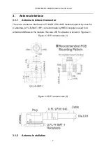
Страница 14: ...antenna interfaces in VT MOD CELL B48 module respectively used for 4 antennas U FL R SMT 1 RF connector made by HRS Company is used for 4 antenna interfaces in the module The size of RF connector is shown in Figure 2 1 Figure 2 1 RF connector size 1 Figure 2 2 RF connector size 2 3 1 2 Antenna Installation ...

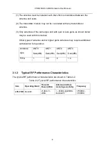
Страница 15: ...odule Other types of antenna and or higher gains antennas may require additional authorization for operation Antenna type ANT0 Gain dBi ANT1 Gain dBi ANT2 Gain dBi ANT3 Gain dBi PIFA 1 0 3 0 1 4 3 1 3 Typical RF Performance Characteristics The typical RF performance characteristics are shown in Table 2 2 Table 2 2 Typical RF performance characteristics Item Operating Band Transmit Power dBm Antenn...

Страница 16: ...mum Ratings VT MOD CELL B48maximum ratings of LTE module is shown in Table 3 1 Table 3 1 VT MOD CELL B48 LTE module absolute maximum rating Parameter Description Minimum Value Maximum Value Unit VCC_3V3 Module Input Voltage 0 3 4 2 V VIN IO Port Input Voltage 0 3 3 6 V Stresses above those listed under Absolute Maximum Ratings may cause permanent damage to the device This is a stress rating only f...

Страница 17: ...r VT MOD CELL B48 are as follows Wherein VDD_IO 1 8V Table 3 3 VT MOD CELL B48 Recommended application conditions Parameter Description Minimum Value Maximum Value Unit VIH High level input voltage 1 26 2 1 V VIL Low level input voltage 0 3 0 54 V VOH High level output voltage VDD_IO V VOL Low level output voltage V 4 5 Power Supply and Consumption 4 5 1 Input Power Supply For VT MOD CELL B48 the ...

Страница 18: ...wn as Table 3 5 Table 3 5 DC power consumption Note 4 Parameter description Min Type Max Unit Band48 550 mA Note 4 Unless specified otherwise the data in the table are obtained in the following test conditions VCC_3V3 3 3VDC T 25 4 5 3 Boot Procedure VT MOD CELL B48 LTE module is booted by loading power VCC_3V3 ...

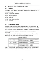
Страница 19: ...etwork The USIM also provides the subscriber s verification procedures as well as authentication methods for network authentication during the attach procedures A class B 3 0 V class C 1 8 V USIM card can be connected to VT MOD CELL B48 module The USIM card interface signals are shown in Table 4 1 Table 4 1 USIM pins PIN Name Description Direction to Module 8 VSIM Power source for the external USI...

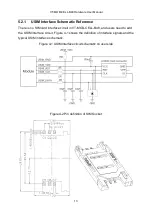
Страница 20: ...s no SIM card interface circuit in VT MOD CELL B48 and users need to add the USIM interface circuit Figure 4 1 shows the definition of interface signals and the typical USIM interface schematic Figure 4 1 USIM interface circuit schematic on user side Figure 4 2 Pin definition of SIM Socket ...

Страница 21: ...VT MOD CELL B48 Hardware User Manual 14 ...

Страница 22: ...nsient signals power supply chokes and DC DC switching FETs _ Avoid routing of these signals near output connectors _ Keep SIM interface signals isolated from other signals 2x width spacing 1 5xmin between SIM interface signals and all other signal routing is recommended Since the SIM is a CMOS device ESD protection devices should be placed near to the SIM connector to provide protection before co...

Страница 23: ...e information the RNDIS interface can be customized 5 5 Status Indication Signals There are four GPIO pins of VT MOD CELL B48module The mode LED functions as the network mode indicator and the status LED function as the signal strength indicator The LEDs are controlled by a sink current source The high voltage is the voltage of VCC3V3 with the typical value of 3 3V According to LED feature you can...

Страница 24: ...ule will be reset Figure 4 4 RESET interface Note 50 ms t 200ms In addition because the pin is rather sensitive to interference it is important to pay attention to the module interface board line otherwise it may bring such as interference caused by module reset 5 7 Recovery Manufacture Configuration A FACT_RST pin provided by VT MOD CELL B48 can recover manufacture configuration through pull low ...

Страница 25: ...nical Specifications This chapter mainly describes mechanical specifications of VT MOD CELL B48 module including VT MOD CELL B48 Overall Dimensions Size 48 0 20 x 44 0 20 x 3 4 0 10 mm Weight 15 0 5 g Figure 5 1 VT MOD CELL B48 overall dimensions ...

Страница 26: ...way from combustible and explosive environment for fear of danger Keep away from all energized circuits Operators should not remove enclosure from the device Only the group or person with factory certification is permitted to open the enclosure to adjust and replace the structure and components of the device Do not change components unless the power cord is removed In some cases the device may sti...

Страница 27: ...his manual Vantron assumes no responsibility of possible missing contents and information errors in contents citations examples and source programs Vantron reserves the right to make necessary changes to this manual without prior notice No part of this manual may be reprinted or publicly released in forms of photocopy tape broadcast e document etc ...

Страница 28: ... that there are no additional unintentional emissions other than what is permitted in Part 15 Subpart B or emissions are complaint with the transmitter s rule s The Grantee will provide guidance to the host manufacturer for Part 15 B requirements if needed End Product Labeling When the module is installed in the host device the FCC ID label must be visible through a window on the final device or i...

Страница 29: ...erates uses and can radiate radio frequency energy and if not installed and used in accordance with the instructions may cause harmful interference to radio communications However there is no guarantee that interference will not occur in a particular installation If this equipment does cause harmful interference to radio or television reception which can be determined by turning the equipment off ...

Страница 30: ...VT MOD CELL B48 Hardware User Manual 23 uncontrolled environment This equipment should be installed and operated with minimum distance 20 cm between the radiator your body ...

Страница 31: ... contact us US Office Vantron Technology Inc Address 440 Boulder Court Suite 300 Pleasanton CA 94566 USA Tel 925 621 8758 Email sales vantrontech com China Office Chengdu Vantron Technology Ltd Address 4th 6th Floor 1st Building No 9 3rd Wu Ke East Street Wu Hou District Chengdu 610045 China Tel 86 28 8512 3930 3931 8515 7572 6320 Email sales vantrontech com cn ...

Отзывы: