at least 60 Log1 O (F/3) dB, and frequen
cies above 20
kHz
by at least 50 dB. Tran
sistor 0208 clamps the output of the
speech amplifier to ground during the re
ceive mode.
Frequency Modulator
The output of the speech amplifier is fed to
the modulator inside the VCO and through
the modulation limit control (VR202) varac
tor diode, 0402. Varactor diode 0402
modulates the reference crystal. The VCO
is frequency modulated by the audio signal
that is applied to it. This modulated RF sig
nal is then applied to the VCO buffer,
0411, before being used as the transmit
frequency or the first receive injection fre
quency.
RF Power Amplifier
The signal, at the proper transmit fre
quency and containing modulation, is fed
to 0201, 0203, and 0205 which operate
as RF amplifiers to provide sufficient drive
level to the RF power amplifier. Transistors
0301, 0302, and 0303 form the RF power
amplifier which increases the output power
to 30 watts. The signal then passes
through a tunedoutput circuit to transform
the collector impedance of Q303 to 50
ohms. The signal is applied to a solid state
transmit/receive switch, 0301, followed by
a lowpass filter that suppresses transmitter
harmonics.
Power Controls
The ALC (Automatic Level Control) circuit
consists of IC 301, 0306, 0307, and
VR301. The ALC monitors the transmitter's
forward power and controls the collector
current to Q301 to maintain 30 watts of out
put power under varying load conditions.
Receiver RF Section
The receive signal is directed to the triple
tuned helical resonator FL 101 by the solid
state transmit/receive switch 0301. The in
put of the receiver is overload protected by
diodes 0801 and 0802. The signal is then
amplified by Q101 and passed through a
triple-tuned helical resonator, FL 102, to the
first mixer.
The first mixer is composed of 0102 and
L 108. The receive VCO frequency is buff
ered by Q103 and filtered by FL 103 before
being fed to the gate of 0102 and mixed
with the received signal to produce the first
I. F. of 45.1
MHz.
First and Second l.F.
The output of the first mixer, at L 108 is
passed through a 45.1
MHz
crystal filter,
FL 105 and tuned inductor L 110, to obtain
the desired selectivity. The signal is then
amplified by 0105 and filtered again by
FL 106 and F112 to improve the selectivity.
The 1.F. signal is then applied to pin 7 of
IC101. This integrated circuit contains the
second mixer and second local oscillator.
A 44,645 MHz crystal, X101, is connected
to pins 1 and 3 of IC101 to complete the
second local oscillator. The output of the
second mixer, is passed through two 455
kHz
ceramic filters, FL 107 and FL 108,
then applied to the amplifiers, limiter and
quadrature detector of IC101. The recov
ered audio is available at pins 10 and 11 of
IC101.
Squelch Gate
The unm uted audio from IC101 pin 10 is
amplified by the noise amplifier, 0106,
then fed to the squelch control, VR752,
through the limit control, VR102, to the ac
tive highpass filter, IC103 2/2. The active
highpass filter, IC103 212, allows the high
frequency "rush" noise to pass. This noise
December 1 992
SMH 4000
Page 1 3
Содержание SMH 4000
Страница 20: ...Page 20 SMH 4000 December 1 992 ...
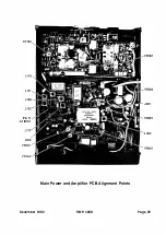
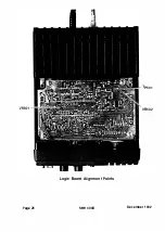
Страница 24: ..._TP601 VR602 Logic Board Alignment Points Page 26 SMH 4000 December 1 992 ...
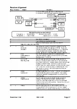
Страница 26: ...Page 28 SMH 4000 December 1 992 ...
Страница 27: ......
Страница 47: ...CC SM 38 Revision 1 SMH 4000 December 1 992 ...
Страница 49: ...SMH 4000 Exploded Mechanical View Page 1 8 S M H 4000 I 0 I 0 0 a 3 December 1 992 ...
Страница 57: ...SMH 4000 Main PCB PD 308BA Solder Side Page 34 SMH 4000 0 Component Side D Solder Side December 1 992 ...
Страница 62: ... I December 1 992 SMH 4000 Earlier Version Logic PCB PD 304AC Component Side SMH 4000 Page 39 ...
Страница 72: ......


