background image

Theory of Operation 

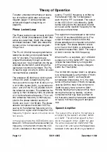
To better understand the theory of opera­

tion of the 

SMH 

4000 refer to the block 

diagram (page 17) and appropriate 
schematic diagrams (beginning on 
page 29). 

Phase Locked Loop 

The Phase Locked Loop consists of IC403 

(PLL I

C

), IC402 (the prescaler), 

0401 

(the 

active low pass filter), 

IC401 

(the voltage 

controlled oscillator, 

X401 

(the reference 

crystal), and a microprocessor program­

ming circuit. 

The PLL IC (IC403) has a programmable 

reference counter, and programmable "N" 
and "A" counters. The counters are 

programmed serially through a common 

data input  (pin 10) and latched into the ap­

propriate counter latch,  according to the 
last data bit (control bit)  entered.  The PLL 
IC has the logic circuitry to control an exter­

nal dualmodulus prescaler. 

The prescaler  (IC402) has a dividing ratio 
of 64 or 65 which  is determined by the 
modulus control output from IC403,  pin 12. 
A 12.8 MHz crystal, 

X401, 

is connected to 

pins 1 and 2 of the PLL 

IC  (IC403) 

to form 

the reference oscillator. This reference fre­

quency  is then divided by 1024,  to produce 

a 12.5 kHz reference frequency. This 12.5 
kHz reference frequency is internally ap­

plied to the phase detector section of 

IC403,  and to pin 

13 

of 

IC403. 

The phase 

detector compares the divided VCO fre­
quency to the  reference frequency and is­
sues an error signal  which  forces the VCO 

frequency higher or lower until a lock condi­

tion occurs. 

In 

the receive mode the 

VCO (IC401) 

oscil­

lates 45.1 

MHz 

above the receive channel 

frequency. In the transmit mode the VCO 

(IC401) oscillates on the transmitting fre-

quency.  The VCO frequency is shifted by 

the data sent from the microprocessor 

each time the PTT is pressed. The output 
of the VCO (IC401)  is buffered by 0205 

before being fed to the prescaler (IC402) 
and used as the injection frequency for the 

receiver and transmitter. 

The signal from the prescaler is fed to the 

"A" and "N" counters 

(IC403, 

pin 8.) The 

output of these counters is fed to the 
phase detector and compared to the refer­
ence signal. The phase detector output, 
pins 15 and 16 of IC403,  is connected to 
the active lowpass filter, 

0401. 

The output 

of 0401 controls the VCO frequency. 

When the PLL is outoflock, pin 7 of 

IC403 

pulses low, turning 0204 OFF;  this in turn, 

inhibits the transmitter by turning 0202 

OFF and removing the supply voltage to 
0203, the TX amplifier. 

The 12.800 

MHz 

crystal  (X401) is tempera­

ture compensated by a thermistor  (TH401) 
and a heater (0407). As the ambient 
temperature drops below -51 C the resis­
tance of the thermistor (TH401) increases, 

causing 0405 to draw more current and 
0406 to supply more current to 0407, 
thereby heating the crystal and thus main­
taining the frequency stability. All other 

components that may have an effect on 
the frequency stability have been selected 

to have a minimal change with tempera­
ture. 

Speech Amplifier 

The output of the dynamic microphone is 
amplified by the speech amplifier, 

0206 

and 

0207. 

The amplified speech is then 

fed to the speech limiter, 

IC201 1/2,  and 

the active lowpass filter 

IC201 2/2.  This 

low pass filter attenuates 

the frequencies 

between 3 

kHz 

and 20 

kHz 

by a factor of 

Page 1 2  

SMH 4000 

December 1 992 

Содержание SMH 4000

Страница 1: ...uniden uniden UNIDEN AMERICA CORPORATION Cellular Communications Division 4700 Amon Carter Blvd Fort Worth TX 76155 817 858 3300 CCSM 38 Revision 1 SMH 4000 150 to 174 MHz SERVICE MANUAL ...

Страница 2: ...ny radio equipment with the antenna touching or close to the eyes face or exposed body parts DO NOT operate the transmitter of any radio equipment unless all the Radio Frequency RF connectors are secure and any open connectors are properly terminated DO NOT operate the transmitter of any radio equipment near electrical blasting caps or in an explosive atmosphere DO NOT let children operate any tra...

Страница 3: ...6AA Component Side 32 Main PCB PD 308BA Component Side 33 Main PCB PD 308BA Solder Side 34 Main PCB PD 308AA Component Side Earlier Version 35 Main PCB PD 308AA Solder Side Earlier Version 36 Logic PCB PD 304AD Component Side 37 Logic PCB PD 304AD Solder Side 38 Logic PCB PD 304AC Component Side Earlier Version 39 Logic PCB PD 304AC Solder Side Earlier Version 40 Power Amplifier PCB PD 309AC Compo...

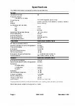
Страница 4: ... Noise Modulation Frequency Response Audio Distortion Receiver ModulationAcceptance Operating Bandwidth without Degradation Sensitivity 20 dB Quieting 1 2 dB Sinad Squelch Selectivity Intermodulation Rejection Frequency Stability Spurious Response Image greater than Audio Output 8 0 A 1 0 A 600 mA 30 C to 60 C 30 kHz 5 0 kHz Synthesized PLL 5 kHz Conforms to EIA RS 1 52 B 40W 24 MHz 0 0005 1 6KOF3...

Страница 5: ...alled Your Uniden Dealer will be able to help you with any or all of these requirements and will be there to help you with all your future communications needs Replacement Parts Replacement parts are available through the Uniden Parts and Service Division lo cated in Indianapolis Indiana When or dering replacement parts please use the complete identification number of the part If the identificatio...

Страница 6: ...smitter s output power frequency and Adverse Vehicle Operation The installation of radio equipment in cer tain vehicles may adversely affect vehicle operations such as Engine performance Driver information systems Anti skid braking systems Electrical charging systems Entertainment systems Uniden America Corporation is not respon sible for the cost to protect the vehicle from adverse operations fol...

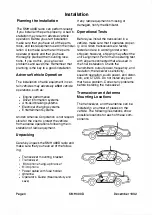
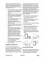
Страница 7: ...nough to fit almost anywhere You can in stall it under the dash seat or in any other convenient location Plan the location for mounting the transceiver so that all con trols and displays can be viewed and easi ly accessed by the operator but the loca tion does not obstruct the driver s vision The antenna cable power cord and the external speaker wiring connect at the rear of the radio The radio ca...

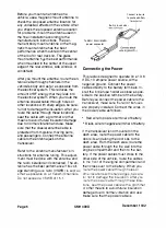
Страница 8: ...a and the radio installed and connected The an tenna has the best performance if its volt age standing wave ratio VSWR is kept as small as possible on all transmit channels Do not exceed a VSWR of 1 5 1 Connect red wire to positive battery terminal Built in fuse holder To SMU 300H K M N power connector Connecting the Power This radio is designed to operate on a 13 6 voe 10 ampere power source with...

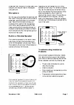
Страница 9: ... pins 1 and 2 of the speaker jumper plug Place the speaker jumper plug in the accessory socket at the rear of the radio 10 7 4 ouu 11 8 5 000 12 9 6 3 0000 WA105 If an external speaker is used make sure that you have the speaker properly con nected to the speaker jumper plug Make sure that you have the speaker s positive wire connected to pin 1 of the speaker jumper plug jumper and the speaker s t...

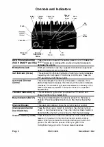
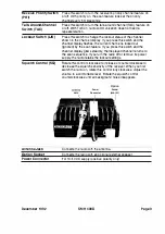
Страница 10: ...ts the intensity of the radio s indicators If tl1e ambient light level increases the intensity of the radio s indicators increases If the ambient light level decreases the intensity of the radio s indicators decreases This control calls for no operator adjustments This red indicator lights when you press the PPT switch and shows that the radio is transmitting This yellow indicator lights if a carr...

Страница 11: ...nnel display flashes the current channel is locked out ignored by the scan feature If you press this switch and the channel display glows steadily the displayed channel returns to the scan sequence If you turn the radio off or remove its power supply the radio retains the lockout settings Rotate this control clockwise to increase or counterclockwise to decrease the squelch sensitivity of the recei...

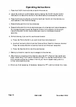
Страница 12: ...ults in decreased receiver sensitivity 6 Do the following if you want to use the scan feature a Press the Priority Switch if you want to set the priority feature on b Use the Channel Up Switch and the Channel Down Switch to choose a channel Press the Lockout Switch to lock the channel out of the scan sequence c Press the Scan Switch to start the scan feature 7 Before you transmit listen for any me...

Страница 13: ...150 MHz to 174 MHz The SMH 400D radio has the following built in features 38 EIA CTCSS Continuous Tone Control Squelch System tones 104 DCS Digital Coded Squelch codes Talk Around Channel 1 Scan Priority channel 36 Scan Lockout Channels Selectable Scan Dwell Time Selectable Dropout Delay Time Time Out Timer 36 programmable receive channels 36 programmable transmit channels For the operator to use ...

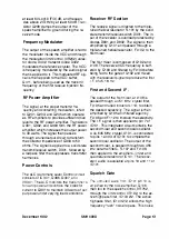
Страница 14: ...el frequency In the transmit mode the VCO IC401 oscillates on the transmitting fre quency The VCO frequency is shifted by the data sent from the microprocessor each time the PTT is pressed The output of the VCO IC401 is buffered by 0205 before being fed to the prescaler IC402 and used as the injection frequency for the receiver and transmitter The signal from the prescaler is fed to the A and N co...

Страница 15: ...itions Receiver RF Section The receive signal is directed to the triple tuned helical resonator FL101 by the solid state transmit receive switch 0301 The in put of the receiver is overload protected by diodes 0801 and 0802 The signal is then amplified by Q101 and passed through a triple tuned helical resonator FL102 to the first mixer The first mixer is composed of 0102 and L108 The receive VCO fr...

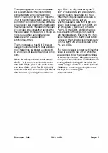
Страница 16: ...oprocessor The anode of D702 is connected to the emitter of 0701 dimmer circuit The DISPLAY LED 0701 receives data from microprocessor pin 54 which is loaded into two shift registers IC752 and IC752 The clock signal for the shift registers is provided by the IC602 pin 52 During the time that the data is being loaded into the shift registers the STB line pin 53 is held low thus preventing the LED f...

Страница 17: ...ives reference counter data 16 bits of data followed by pulsing the enable line high IC601 pin 57 followed by the N and A counter data 20 bits of data fol lowed by pulsing the enable line high When the microprocessor sends data to the DISPLAY LED it is sent as synchronous serial data from IC601 pin 54 with clock pulses sent from IC601 pin 52 While data is being sent to the DIS PLAY LED the IC601 p...

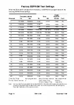
Страница 18: ...none Yes 11 none 160 160 none none none Yes 12 none 160 180 none none none Yes 13 none 160 200 none none none Yes 14 none 160 220 none none none Yes 15 none 160 240 none none none Yes 16 none 160 260 none none none Yes 17 none 160 280 none none none Yes 18 none 160 300 none none none Yes 19 none 160 320 none none none Yes 20 none 160 340 none none none Yes Time Out Timer Not programmed Busy Channe...

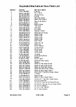
Страница 19: ...SCW803008N HBCT382392Z SSCW235025N SSCW293508N SSCW490050N SSCW530035N SSCW540050N December 1 992 Part Description Chassis FrontPanel Display Plate Handle Mounting Screw Black Push Button Gray Push Button Knob Bottom Case Top Case IC Holder IC Holder Speaker Holder Microphone Hanger Shield Plate Shield Plate ShieldPlate Shield Plate Earth Plate Antenna Lug Earth Lug Brand Badge ControlPlate LED Ho...

Страница 20: ...Page 20 SMH 4000 December 1 992 ...

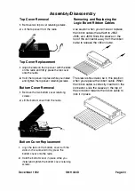
Страница 21: ...e bottom cover with the slots on the radio and firmly press the bottom cover onto the radio 2 Hold the bottom cover in place while you install and tighten the bottom cover retaining screws Removing and Replacing the Logic Board Ribbon Cables Use caution when you remove or replace the ribbon cables that attach to J602 J605 and J606 Slide the sleeve on the top of the connector away from the ribbon c...

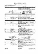
Страница 22: ...ce Ocillator VR401 CTCSS Deviation AF SiO lal Generator VR202 Voice Deviation VR601 CTCSS Deviation VR201 Total Deviation Key transmitter and verify that reading on power meter does not exceed 50 watts Adjust VR301 if necessary Typical power meter readings for channels 1 2 and 3 should be Channel 1 48 watts Channel 2 42 watts Channel 3 38 watts Key transmitter and adjust L402 for 1 50 505 M Hz 200...

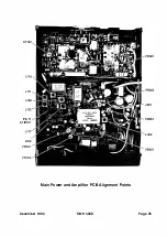
Страница 23: ...CT301 L111 Pin 11 of IC101 L109 VR101 VR102 Main Power and Amplifier PCB Alignment Points December 1 992 SMH 4000 VR301 J201 VR201 L402 Page 25 ...

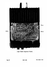
Страница 24: ..._TP601 VR602 Logic Board Alignment Points Page 26 SMH 4000 December 1 992 ...

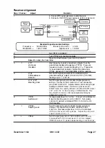
Страница 25: ...645 MHz 50 Hz reading Set the RF signal generator to the standard signal generator settings Adjust L1 09 for 2 6 VDC 0 5 VDC reading at pin 1 1 of IC1 02 Set RF signal generator to standard signal generator settings Connect SINAD meter to 8 n load connecting pins 2 and 3 of WA1 01 Adjust volume control until you get reading on SINAD meter Decrease signal level until SINAD meter has reading between...

Страница 26: ...Page 28 SMH 4000 December 1 992 ...

Страница 27: ......

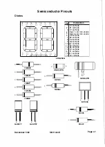
Страница 28: ...1 cathode 3 D1 cathode F2 4 Digit 1 common anode 5 Digit 2 common anode 6 D2 cathode 7 E2 cathode G2 8 C2 cathode 9 G2 cathode 1 0 A2 cathode E2 1 1 F2 cathode 1 2 82 cathode 02 1 3 81 cathode 1 4 F1 cathode _ 1 5 A1 cathode 5 6 7 8 1 6 G1 cathode LDG202A c 11 I A ii IJ C HSK1 20TR c c Q Q Q A Q Q 0 CD II 1 g c A 2 Ol Qi i HZKGCTR I A HZ7A3 c A A HZ9C2 A A c A KV1 330 c I I A Ml308 c II A Ml407 SM...

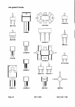
Страница 29: ...B 2 81 1 43 Page 48 0 B C E 2SB891 B E C 2SC2026 B E C 2SC2407 B E C 2SC2538 E GND 0 E 2SC2539 E C B 2SC2673 2SC2694 c c E Q G N D E W W B E B E 2SC271 2 2SC2714 SMH 4000 Marking Side B C E 2SC3337 c B E 2 01 048 D c 5 0 Cf 2SK302 c w B E DTC1 44EK B MRF553 December 1 992 ...

Страница 30: ...1 5 NC 1 1 14 LIM OUT 12 1 3 QUAD I N CXA1 003AM 5 GND _ _ _ ___ CXK1 013P December 1 992 0 1 2 0 0 I z I 0 CL CL z l o u 0 MB87006A co 0 1 z 0 M51 951 AML 0 3 4 5 6 0 7 8 I I I I I I I I j I j I u CL 0 w z CD z u z I LL 0 z I 0 I 0 0 0 co MB371 2 I P 1 0 B I P Vee 2 7 CD SW 3 O P 4 MB504P SMH 4000 OSCin 0R OSCout 0V fv RE Fout Vdd 4 fr Modulus Control Vss LE LD 1 0 Data 9 Clock MB87006A N I NV2 1...

Страница 31: ...2 7 P6 0 56 P0 0 P4 7 AN 7 1 0 55 P0 1 P4 6 AN 6 1 1 54 P0 2 P4 5 AN 5 1 2 53 P0 3 P4 4 AN 4 1 3 52 P0 4 P4 3 1 4 5 1 P0 5 P4 2 1 5 50 P0 6 P4 1 1 6 49 P0 7 P4 0 1 7 48 P 1 0 P3 7 1 8 47 P1 1 P3 6 1 9 46 P1 2 P3 5 45 P1 3 P3 4 44 P1 4 P3 3 CNTR 43 P1 5 P3 2 INT 2 42 P 1 6 P3 1 4 1 P 1 7 P3 0 40 PS 0 INT 1 39 PS 1 CNVss 38 P5 2 RESET 37 P5 3 Xin 36 P5 4 ED 4 Xout 35 P5 5 ED 5 0 3 1 34 P5 6 ED 6 Vss...

Страница 32: ... 025Z CC 0 001 µF 50V K B C 1 40 PD 308AC C 1 04 BCVP81 1 025Z CC 0 001 µF 50V K B C 1 40 PD 308AC C 1 05 BCVM81 1 204Z CC 1 2PF 50V J CH C 1 40 PD 308AC C 1 07 BCVL81 2704Z CC 27PF 50V J SL C 1 40 PD 308AC C1 09 BCVP81 1 025Z CC 0 001 µF 50V K B C 1 40 PD 308AC C1 1 0 BCVQ31 1 036Z CC 0 01 µF 1 6V M Y C 1 40 PD 308AC C1 1 1 BCVQ31 1 036Z CC 0 01 µF 1 6V M Y C 1 40 PD 308AC C1 1 2 BCVM81 1 204Z CC...

Страница 33: ... C 1 40 PD 308AC C21 7 BCXE81 3335Z CC 0 033 µF 50V K C B PD 308AC C21 8 BCVP81 1 025Z CC 0 001 µF 50V K B C 1 40 PD 308AC C220 BCVP81 1 025Z CC 0 001 µF 50V K B C 1 40 PD 308AC C221 BCXS51 1 045Z CC 0 1 µF 25V K B PD 308AC C222 BCVPB1 1 025Z CC 0 001 µF 50V K B C 1 40 PD 308AC C223 BCER81 1 096Z EL 1 µF 50V M C 095 PD 30BAC C225 BCXEB1 3335Z CC 0 033 µF 50V K C B PD 308AC C226 BCER31 1 006Z EL 1 ...

Страница 34: ... CC 82PF 500V J C 073 PD 309AB C331 BCDD823304Z CC 33PF 500V J C 073 PD 309AB C332 BCDD823304Z CC 33PF 500V J C 073 PD 309AB C333 BCXE81 2225Z CC 0 0022 µF 50V K C B PD 309AB C335 BCXE81 2225Z CC 0 0022 µF 50V K C B PD 309AB C336 BCXE81 2225Z CC 0 0022 µF 50V K C B PD 309AB C337 BCXE81 2225Z CC 0 0022 µF 50V K C B PD 309AB C340 BCDD821 204Z CC 1 2PF 500V J C 073 PD 309AB C341 BCDD821 204Z CC 1 2PF...

Страница 35: ...25Z CC 0 001 µF 50V K B C 1 40 PD 308AC C435 BCER9022062 EL 22 µF 6 3V M C 095 PD 308AC C436 BCVP81 1 025Z CC 0 001 µF 50V K B C 1 40 PD 308AC C437 BCA251 1 026Z EL 1 000 µF 25V M C 1 56 PD 308AC C438 BCXE81 1 0352 CC 0 01 µF 50V K C B PD 308AC C440 BCAZ51 1 026Z EL 1 000 µF 25V M C 1 56 PD 308AC C443 BCER1 1 1 01 6Z EL 1 00 µF 1 0V M C 095 PD 308AC C445 BCER51 1 0062 EL 1 0 µF 25V M C 095 PD 308A...

Страница 36: ...39006 JK 039 3022 06A PD 304AC J701 BJKY0420001 JK 420 PD 305AB SK601 BSKY0047064 SK 047 DICS 64C 64P P0 304AC Crystals Symbol Part Number Description Board Number s X1 01 BQXY0271 001 QX 271 44 645 MHz PD 308AC X401 BQXY01 58002 QX 1 58 1 2 800 M Hz PD 308AC X601 BQXY0281 002 QX 281 4 1 904 M Hz P0 304AC Diodes Symbol Part Number Description Board Number s 01 20 BOAY0001 002 1 N60 P P0 308AC 0 1 ...

Страница 37: ...0624001 LB 624 1 99KC 1 5097ZW PD 308AC L1 1 4 BLZY0051 478 LZ 051 SP0305 R47M 0 47 µH PD 308AC L1 1 7 BLBY0232001 LB 232 1 1 3KN 6546Z PD 308AC L1 1 8 BLZY0051 1 01 LZ 051 SP0305 1 01 K 1 00 µH PD 308AC L1 20 BLZY0051 1 01 LZ 051 SP0305 1 01 K 1 00 µH PD 308AC L1 21 BLZY001 6471 LZ 01 6 SL0609 471 K 470 µH PD 308AC L1 25 BLZY00501 08 LZ 050 0 1 µH PD 308AC L1 26 BLOY0236001 L0 236 1 59SNSF 1 372 ...

Страница 38: ... 01 BOEY0947001 IC CXA1 003AM P0 308AC IC1 02 BOEY0802001 IC UC1 1 05 P0 308AC IC1 03 BDEY1 1 95001 IC NJM4560S P0 308AC IC1 05 BOEY01 57001 IC MB3712 P0 308AC IC201 BDEY0464001 IC BA71 5 P0 308AC IC301 BDEY0703001 IC NJM2904M P0 309AB IC401 BOEY1 077001 IC UC 1 1 67 P0 308AC IC402 BDEY0462001 IC MB504P P0 308AC IC403 BOEY0674002 IC MB87006A P0 308AC IC405 BOEY0397001 IC NJM7808A P0 308AC IC406 BO...

Страница 39: ...CB Control PCB Logic PCB 0 Type MF Metal Film RC Resistor Chip RT Trimmer Resistor RV Variable Resistor Description RC 2 7K n 1 8W J RC 2 7K n 1 8W J RC 1 2 n 1 8W J RC 1 00 n 1 8W J RC 3 3K n 1 8W J RC 1 K n 1 8W J RC 330 n 1 8W J RC 1 5K n 1 8W J RC 56 n 1 8W J RC 5 6K n 1 8W J RC 1 K n 1 8W J RC 1 00 n 1 8W J RC 1 00 n 1 8W J RC 5 6K n 1 8W J RC 330K n 1 8W J RC 1 5K n 1 8W J RC 1 5K n 1 BW J R...

Страница 40: ... PD 308AC R223 BRFD1 86834Z RC 68K n 1 8W J PD 308AC R224 BRFD1 81 024Z RC 1 K n 1 8W J PD 308AC R225 BRFD1 81 034Z RC 1 0K n 1 8W J PD 308AC R226 BRFD1 81 234Z RC 1 2K n 1 8W J PD 308AC R227 BRFD1 81 234Z RC 1 2K n 1 8W J PD 308AC R228 BRFD1 82724Z RC 2 7K n 1 8W J PD 308AC R230 BRZY0021 001 RZ 021 JC2A PD 308AC R231 BRFD1 86824Z RC 6 8K n 1 8W J PD 308AC R232 BRFD1 84744Z RC 470K n 1 8W J PD 308...

Страница 41: ...406 BRFD1 81 034Z RC 1 0K n 1 BW J PD 308AC R407 BRFD1 81 01 4Z RC 1 00 n 1 8W J PD 308AC R408 BRFD1 82224Z RC 2 2K n 1 8W J PD 308AC R409 BR FD1 83934Z RC 39K n 1 8W J PD 308AC R41 0 BRFD1 84734Z RC 47K n 1 8W J PD 308AC R41 1 BRFD 1 84734Z RC 47K n 1 8W J PD 308AC R41 2 BRFD1 84724Z RC 4 7K n 1 8W J PD 308AC R41 3 BRFD1 81 024Z RC 1 K n 1 8W J PD 308AC R41 4 BRFD1 839342 RC 39K n 1 8W J P0 308AC...

Страница 42: ...F 5 6K a 1 6W J CF 1 8K Q 1 6W J CF 1 OOK Q 1 6W J RC 1 0 Q 1 8W J RC 1 0K a 1 8W J RC 1 0K Q 1 8W J RC 1 0K Q 1 8W J RC 5 6K Q 1 8W J RC 1 0K Q 1 8W J RC 470 n 1 8W J RC 1 K n 1 8W J RC 470 n 1 8W J RC 1 0K n 1 8W J RC 1 0K n 1 8W J RC 1 0K n 1 8W J RC 1 0K a 1 8W J RC 1 0K n 1 8W J RC 33K n 1 8W J RC 1 K n 1 8W J RC 1 0K n 1 8W J RC 1 0K n 1 8W J RC 1 0K n 1 8W J RC 1 0K n 1 8W J RC 1 0K Q 1 8W ...

Страница 43: ...90 n 1 1 0W J PD 305AB R703 BRFC0 1 39 1 4Z RC 390 n 1 1 0W J PD 305AB R705 BRFC0 1 39 1 4Z RC 390 n 1 1 0W J PD 305AB R706 BRFC01 391 4Z RC 390 n 1 1 OW J PD 305AB R707 BRFC0 1 39 1 4Z RC 390 n 1 1 0W J PD 305AB R708 BRFC0 1 39 1 4Z RC 390 n 1 1 0W J PD 305AB R71 0 BRFC01 39 1 4Z RC 390 n 1 1 OW J PD 305AB R71 1 BRFC0 1 391 4Z RC 390 n 1 1 0W J PD 305AB R71 2 BRFC01 39 1 4Z RC 390 n 1 1 OW J PD 3...

Страница 44: ...271 2 1 24 DB 381 2SC271 2 Y PD 309AB 0403 BD8C271 2 1 24 08 381 2SC271 2 Y P0 308AC 0405 BD8C271 2 1 24 08 381 2SC271 2 Y PD 308AC 0406 808A1 1 62 1 24 08 036 2SA1 1 62 Y PD 308AC 0407 80880891 1 1 6 08 1 1 6 28889 1 0 PD 308AC 0408 BD8A09501 24 08 01 0 2SA950 Y PD 308AC 041 0 8D8A09501 24 08 01 0 2SA950 Y P0 308AC 041 1 BOBC271 41 1 4 DB 71 8 2SC271 4 0 PD 308AC 041 2 80881 1 431 1 9 08 1 28 288...

Страница 45: ...3 RT 528 1 OKB n PD 308AC VR202 BRTY0528224 RT 528 220KB n PD 308AC VR301 BRTY0528474 RT 528 470KB n PD 309AB VR401 B RTY0527223 RT 527 H0521A1 1 5 22K n PD 308AC VR601 BRTY0531 1 03 RT 531 TMC4K 1 0KB n PD 304AC VR602 BRTY0531 474 RT 531 470KB n PD 304AC VR751 BRVY0674001 RV 674 1 0KA n PD 306AA VR752 BRVY0673001 RV 673 1 OKB n PD 306AA Page 64 SMH 4000 December 1 992 ...

Страница 46: ...Warranty Consult your Uniden Commercial CommunicationsPricing Information for details about the warranty for this unit ...

Страница 47: ...CC SM 38 Revision 1 SMH 4000 December 1 992 ...

Страница 48: ... AF AMP VOLUME 0 1 70 01 07 MUTE SW RX AUDIO MUTE SW I SPEAKER SP208 I 5V 0408 TX RX SWITCH PRESCALER r i I I I I L L L L L ___ I I I I I IC607 0608 RESET IC406 5V REG IC405 BV REG TX B 0410 L WITCHING L r J 1 0402 I I I I J 041 7 SkHz SHIFT IC601 C P U 0403 0405 7 041 2 IC751 LED DRIVER X TAL TEM P 1 1 3 6V SW 14 _ _ IC201 112 IC201 212 PRE EMPH FILTER 0206 207 LIMITER MIC AMP I I IC202 I I I 020...

Страница 49: ...SMH 4000 Exploded Mechanical View Page 1 8 S M H 4000 I 0 I 0 0 a 3 December 1 992 ...

Страница 50: ...l 1 0 llF 0 6 1 K L 5 5 5 F C I 0 3 _ L w _ F_ o _ e_ o_ K _ s_ 5 _ s _ s __ 120 iiLK 3 i 0 0 3 F C I 0 1 I F 2 1 7 F C I O S W F 0 8 3 K 7 0 5 5 P C I O I P D 3 0 8 1 TOP I PCGOI P 0 3 0 L I TOP I VOI O I VZ 665 11 11 1 0 1 R E D 5 2 1 0 3 V l 0 2 REP 5 1 1 0 3 11oin2 llZ 682 WA I O I 11 0 1 1 4 03 e e e 8 8 VOOOI VZ 653 L 1 YE H llT 1 1 0 _ I SMH 4000 Wiring Diagram ...

Страница 51: ...I JP 1 7 1 SMH 4000 E Wiring o1 arher Version agram s Page 22 SMH 4000 W l l O VI 03 BLX 3 180 5 ll L 3 100 5 r I i I I 1 1 I ij l December 1992 f SOUYE RINq Wf IOI Wj G65 9LI AE O HL 130 JHT 1 10 Ell 1 10 ...

Страница 52: ...Y r 7i 0206 2SC2 1 1 2Y I I I I I I I UT8 0 17 2 lJH l H3 C UG AJll AlU Jlf2 JlHI I I I I I I I I I I I I I I I I I I I I I I I I I I I I I 3 1 1 2 lf1 J T 3 UJ i UW l H _ _ 2 3 1 _ 1 _ 2 _ Y _ _ _ _ W r fr _ _ _ _ __ _ _ _ _ f Jr 1 a l 0 3 06 250 1 1 0 T t 111 C t J l J ICJO I NJH290 H 1 2 I j I I I L _ _ _ J lllH 1 1 1 t i 1 t 1 t t 1 I t 1 t t 1 1 t 1 t I t 1 1 I d a I g a i c t I r 1 I I I I I...

Страница 53: ... I I I I I i I I I I I I I I I I I I I i I I l E lier Versions SMH 4000 ar Amplifier PCB Main PCB P wer Schematic D agram Page 30 SMH 4000 0105 SC3337 01 02 2SK302Y It ll5t CJOO L l J O o OllC ItJ01 I 1 I lfJOO I 1 l I ITT r n 03 9 o iCjOt HRF553 NJH2904H 1 2 NJH2904H 212 oecenlb9r1992 I I I I I I a a 0 3 u 1 i 9 d R lotl _ _ _ _ _ _ _ I I I I I I I I I I I I I 1 2I f I JSOI 1 I ia _5 1 j L_ _ _ _...

Страница 54: ...svs 11 c let c 060 4 OTCl l EK I OC IS _ _ I l s _ E St ltl S tl o s 1 11 r _ T r OTg i 1 c c c 1 u s I 0 7 0 1 1 1 T ti 25C267 30 2 13 Q J 2 060 1 r D H l 4 __ D1tl LDCltlt 1 C 1 t 0603 u OTCl EK r 11 45 _ 11 m11 DTCIUEX f T c D c I i 1 11t I _ _ I I I I I C607 H51 951 AHL 0 c r CD c 0608 c c s II iis H r _ _q i l 131 CD S 1 I _ 2 I a r I I r t 1 1 1 M j 1 4 __ _ __ 2 s 5 c t c t E r II 14 R U II...

Страница 55: ...SMH 4000 Switch PCB P0 306AA Component Side Page 32 SMH 4000 December 1 992 SMH 4000 Front PCB P0 305AB Component Side SMH 4000 Front PCB P0 305AB Solder Side PATT E Rt 1 c u 1 ...

Страница 56: ...TOUCHER 1 1 4 8 1 938 D Component Side D Solder Side December 1 992 SMH 4000 SMH 4000 Main PCB PD 308BA Component Side Page 33 ...

Страница 57: ...SMH 4000 Main PCB PD 308BA Solder Side Page 34 SMH 4000 0 Component Side D Solder Side December 1 992 ...

Страница 58: ... D Component Side D Solder Side December 1 992 SMH 4000 Earlier Version Main PCB PD 308AA Component Side SMH 4000 Page 35 ...

Страница 59: ...P C 1 0 l P D 3 0 8 A A J B O r ro11 YJ EW 1 I 0 er SMH 4000 Earlier Version Main PCB PD 308AA Solder Side Page 36 SMH 4000 D Component Side D Solder Side December 1 992 _ ...

Страница 60: ... CI 4_ _ _A t _ l o 1 7 U _ _ _ _ _ _ _ _ _ _ _ _ _ j t o i H JPGdJ J PG31 December 1 992 f f r d r1 d j 5 j i 1 SMH 4000 SMH 4000 Logic PCB PD 304AD Component Side Page 37 ...

Страница 61: ...4000 Logic PCB PD 304AD Solder Side Page 38 C 6 2 7 D SMH 4000 0603 Pt December 1 992 r 0 0 D a R681 CJ CJ RS88 _ r w 0 f a ct a cofl pt _ __ _ _ __ _C J ____ __ _ _ o o _ _ _ _ _ rl o u Lr L _ u R686 1 D _ ...

Страница 62: ... I December 1 992 SMH 4000 Earlier Version Logic PCB PD 304AC Component Side SMH 4000 Page 39 ...

Страница 63: ...n ogic PCB PD 304AC older Side age 40 SMH 4000 December 1 992 h_ r i J i t A Rf i 28 t J 0 6 0 7 u 1 w i_ t v t _ Q j oL c _ c _ _ dltt J N i J D t D lJ er J 6Bf _ 71 _ t i oD J 1 nr t r ii t1 j i J f d iif l 1 r t n J 1 i X r ...

Страница 64: ...l 306 t J i 1 fi t f m I tt 0 I II D Component Side D Solder Side December 1 992 SMH 4000 Power Amplifier PCB PD 309AC Component Location Component Side SMH 4000 Page 41 ...

Страница 65: ...SMH 4000 Power Amplifier PCB PD 309AC Chip Location Component Side Page 42 SMH 4000 D Component Side f Solder Side December 1 992 c C M I J_ ...

Страница 66: ...0306 J IJ I fl 0 U II D Component Side D Solder Side December 1 992 SMH 4000 Earlier Version Power Amplifier PCB PD 309AB Component Location Component Side SMH 4000 Page 43 ...

Страница 67: ...SMH 4000 Earlier Version Power Amplifier PCB PD 309AB Chip Location Com ponent Side Page 44 SMH 4000 D Component Side Ell Solder Side December 1 992 ...

Страница 68: ...D Component Side D Solder Side December 1 992 SMH 4000 Earlier Version Power Amplifier PCB PD 309AA Component Location Component Side SMH 4000 Page 45 ...

Страница 69: ...SMH 4000 Earlier Version Power Amplifier PCB PD 309AA Chip Location Component Side Page 46 SMH 4000 D Component Side D Solder Side December 1 992 ...

Страница 70: ...SMH 4000 Earlier Version Power Amplifier PCB PD 309AA Chip Location Component Side Page 46 SMH 4000 0 Component Side 0 Solder Side December 1 992 ...

Страница 71: ...FOÎÍP EB NBRVJOB FOUSF FN DPOUBUP QFMP FNBJM BMFYBOESF UBCBKBSB HNBJM DPN UBNCFN Ï QJY 0CSJHBEP B UPEPT RVF BKVEBSBN BUF BRVJ 0T TJUFT POEF FTTFT TDBOT QPEFN TFS FODPOUSBEPT XXX CBNB PSH IUUQ UBCBKBSB MBCT CMPHTQPU DPN IUUQ UBCBMBCT DPN CS FTRVFNBUFDB IUUQT EBUBTTFUUF PSH 5 0 4 1 4 3 0 45 0 9 5 5 0 0 0 6 0 0 5 70 5 4 70 10 3 13 3 6 6 5 0 0 03 0 45 5 0 1 6 0 6 JTUSJCVJÎÍP 3 56 5 3FTQFJUF P NFV USBC...

Страница 72: ......
Отзывы: