SARA-R42 - Application note
UBX-20050829 - R02
Testing
Page 42 of 58
C1-Public
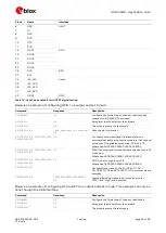
Example of grouping TX and RX tests in non-signaling RF mode:
Command
Response
Description
AT+UTEST=3,123060,23,,,5000
+UTEST: 123060,23,5,1,5000
OK
TX test on B12, Ch. 123060, 23 dBm, 5 s on.
AT+UTEST=3,123095,23,,,5000
+UTEST: 123095,23,5,1,5000
OK
TX test on B12, Ch. 123095, 23 dBm, 5 s on.
AT+UTEST=3,120000,23,,,1000
+UTEST: 120000,23,5,1,1000
OK
TX test on B4, Ch. 120000, 23 dBm, 1 s on.
AT+UTEST=3,120100,23,,,1000
+UTEST: 120100,23,5,1,1000
OK
TX test on B4, Ch. 120100, 23 dBm, 1 s on.
AT+UTEST=2,105020,2000
+UTEST: 105020,2000,0,-20,-20,-19
OK
RX test on B12, Ch. 105020, 23 dBm, 2 s on
2
.
AT+UTEST=2,105070,2000
+UTEST: 105070,2000,0,-21,-20,-20
OK
RX test on B12, Ch. 105070, 23 dBm, 2 s on
1
.
AT+UTEST=2,102000,2000
+UTEST: 102000,2000,0,-21,-20,-20
OK
RX test on B4, Ch. 102000, 23 dBm, 2 s on
1
.
AT+UTEST=2,102100,2000
+UTEST: 102350,2000,0,-21,-20,-20
OK
RX test on B4, Ch. 102350, 23 dBm, 2 s on
1
.
10.1.4
UTEST RF TX non-signaling continuous mode
For TX non-signaling mode, avoid using continuous mode if possible due to the internal mode TX flag
not getting cleared when transitioning to the next non-signaling test.
If the continuous mode is used, then issue a subsequent non-continuous mode of the same frequency,
channel, and power output to clear an internal flag.
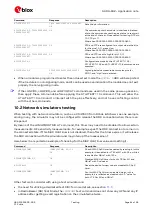
Example of clearing an internal flag if the continuous mode is used for RF TX non-signaling mode:
Command
Response
Description
AT+UTEST=3,123060,23,,,0
OK
Turn on the continuous TX in B12, Ch. 123060, 23
dBm.
AT+UTEST=3,123060,23,,,1000
+UTEST: 123060,23,5,1,1000
OK
Turn on TX for 1 s in B12, Ch. 123060, 23 dBm This will
clear the internal TX flag set by continuous mode.
10.1.5
Digital test
This test mode can be used during OEM production testing to check the correct behavior of the
module’s digital pins and detect possible soldering or functional problems.
The
+UTEST
AT command can be used to configure a specific group of pins as:
•
Digital input: once configured, it is possible to apply a voltage level to the pin.
•
Digital output: the pin can be used to output a digital “high” or “low” voltage level.
Pins enabled for digital testing can be considered as generic digital input / output pins; it is possible
to configure a pin as a dig
ital output with “high” logic level and then verify the voltage level present at
the pin. Conversely, it is possible to apply a “high” or “low” logic level on a pin set as a digital input, and
then check if the module can correctly measure the voltage level applied.
reports number and type of pins available for digital testing via the
+UTEST
AT command.
For a detailed description of the input / output levels characteristics of the pins, see the SARA-R4
series data sheet
2
Use 100 kHz offset from center frequency of RF input signal. For example, to test EARFCN=2525 of LTE B5, corresponding
to 881.50 MHz, set the RF frequency of the generator to 881.50 + 0.1 = 881.6 MHz. Modulation setting is not required.


