ODIN-W2 series - System integration manual
UBX-14040040 - R20
Design-in
Page 25 of 43
C1-Public
3.3.2
Generic digital interfaces supply output (V_INT) design
The ODIN-W2 series modules provide a 1.8 V supply rail output through the V_INT pin. The same
voltage domain is used internally to supply the generic digital interfaces of the modules. The V_INT
supply output can be used for interface logic. The External digital interface logic should have
decoupling on the supply pins according to the respective datasheet.
•
Do not apply loads, which might exceed the limit for maximum available current from V_INT supply
(see the
ODIN-W2 series Data sheet [2]) as this can cause malfunctions in internal circuitry.
•
Since the V_INT supply is generated by an internal switching step-down regulator, it is not
recommended to supply sensitive analog circuitry without adequate filtering for digital noise.
•
V_INT can only be used as an output. Do not connect any external supply source on V_INT.
•
If the line is externally accessible, a higher ESD protection level could be required and it can be
achieved by mounting an ESD protection (for example, EPCOS CA05P4S14THSG varistor array)
close to the accessible point.
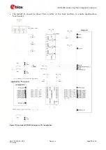
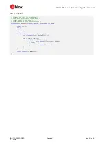
See Schematic for ODIN-W2 section for V_INT design examples.
3.4
Data communication interfaces
3.4.1
Asynchronous serial interface (UART) design
The layout of the UART bus should be done so that noise injection and cross talk are avoided. See the
Schematic for ODIN-W2 section for additional information.
It is recommended to use the hardware flow control with RTS/CTS to prevent temporary UART buffer
overrun.
•
If CTS is 1, then the Host/Host Controller is allowed to send.
•
If CTS is 0, then the Host/Host Controller is not allowed to send.
3.4.2
Ethernet (RMII+SMI)
It is recommended to route all signals in the RMII bus with the same length and have appropriate
grounding in the surrounding layers; total bus length should also be minimized. The layout of the RMII
bus should be done so that crosstalk with other parts of the circuit is minimized providing adequate
isolation between the signals, the clock and the surrounding busses/traces.
Termination resistors are recommended on the RX and TX lines of the RMII bus.
Pull-up resistor is required for MDIO.
The General High Speed layout guidelines in section 3.6 apply for the RMII and the SMI bus.
3.5
Other interface and notes
3.5.1
Low power clock (LPO_CLK) design
The LPO_CLK input pin requires accurate layout design. Avoid injecting noise on these pins as it may
affect the stability of the LPO timing reference. See the Schematic for ODIN-W2 section for additional
information.
3.6
General High Speed layout guidelines
These general design guidelines are considered as best practices and are valid for any bus present in
the ODIN-W2 series modules; the designer should prioritize the layout of higher speed busses. Low
frequency signals are generally not critical for layout.

