LENA-R8 series - System integration manual
UBX-22015376 - R02
Design-in
Page 91 of 116
C1-Public
to an external host processor if their functions are required by the application, otherwise they can be
left unconnected in the application board.
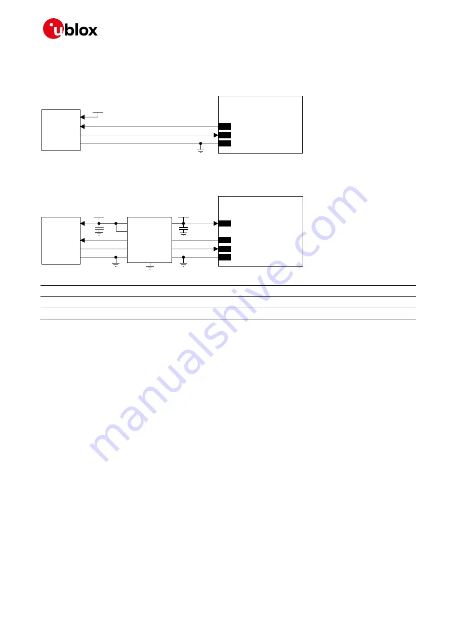
In case 1.8 V external processor, the GNSS PIOs can be directly connected as illustrated in
LENA-R8001M10
46
EXTINT
45
TIMEPULSE
Output
Input
GND
GND
Application
Processor
VCC
1V8
Figure 71: Application circuit for LENA-R8001M10 GNSS PIOs with 1.8 V external host application processor
In case 3 V external processor, the GNSS PIOs have to be connected using proper voltage translator
as illustrated in
LENA-R8001M10
46
EXTINT
45
TIMEPULSE
Output
Input
GND
GND
Application
Processor
VCC
1V8
B1
A1
GND
U1
B2
A2
VCCB
VCCA
C1
C2
3V0
DIR1
DIR2
OEn
99
VCC_GNSS
Unidirectional
Voltage Translator
Figure 72: Application circuit for LENA-R8001M10 GNSS PIOs with 3 V external host application processor
Reference
Description
Part number - manufacturer
C1, C2
100 nF Capacitor Ceramic
Various Manufacturers
U1
Unidirectional Voltage Translator
SN74AVC2T245
- Texas Instruments
Table 50: Components for LENA-R8001M10 GNSS PIOs with 3 V external host application processor
☞
As long as
VCC_GNSS
is not supplied, the GNSS UART pins cannot be driven by an external host
processor. If driving the GNSS UART pins cannot be avoided, buffers are required for isolating the
GNSS UART pins.
☞
For more information and examples about GNSS PIOs external circuit guidelines, see the u-blox
M10 standard precision GNSS chip data sheet
and integration manual
2.13
Module placement
Optimize placement for a minimum length of RF line and a closer path from the DC source for
VCC
.
Make sure that the module, RF and analog parts / circuits are clearly separated from any possible
source of radiated energy, including digital circuits that can radiate some digital frequency harmonics,
which can produce Electro-Magnetic Interference affecting module, RF and analog par
ts / circuits’
performance or implement proper countermeasures to avoid any possible EMC / EMI issue.
Routing of noisy signals below the module, on the top layer of the host PCB, is not recommended.
Make sure that the module, RF and analog parts / circuits, high speed digital circuits are clearly
separated from any sensitive part / circuit which may be affected by Electro-Magnetic Interference or
employ countermeasures to avoid any possible Electro-Magnetic Compatibility issues.
Provide enough clearance between the module and any external part.
☞
The heat dissipation during continuous transmission at maximum power can significantly raise
the temperature of the application base-board below the LENA-R8 series modules: avoid placing
temperature sensitive devices close to the module.


