


SARA-G3 series - System Integration Manual
UBX-13000995 - R06
Objective Specification
Design-in
Page 115 of 218
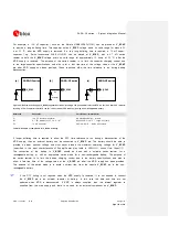
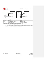
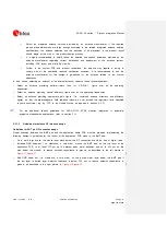
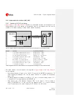
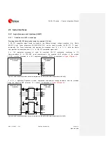
35 um
35 um
1510 um
L2 Copper
L1 Copper
FR-4 dielectric
1200 um 400 um
400 um
Figure 39: Example of 50
coplanar waveguide transmission line design for the described 2-layer board layup
If the two examples do not match the application PCB layup, the 50
characteristic impedance calculation
can be made using the HFSS commercial finite element method solver for electromagnetic structures from
Ansys Corporation, or using freeware tools like AppCAD from Agilent or TXLine from Applied Wave
Research, taking care of the approximation formulas used by the tools for the impedance computation.
To achieve a 50
characteristic impedance, the width of the transmission line must be chosen depending
on:
the thickness of the transmission line itself (e.g. 35 µm in the example of
the thickness of the dielectric material between the top layer (where the transmission line is routed)
and the inner closer layer implementing the ground plane (e.g. 270 µm in
the dielectric constant of the dielectric material (e.g. dielectric constant of the FR-4 dielectric material
in
the gap from the transmission line to the adjacent ground plane on the same layer of the transmission
line (e.g. 500 µm in
, 400 µm in
If the distance between the transmission line and the adjacent GND area (on the same layer) does not
exceed 5 times the track width of the micro strip, use the “Coplanar Waveguide” model for the 50
calculation.
Additionally to the 50
impedance, the following guidelines are recommended for the transmission line
design:
Minimize the transmission line length: the insertion loss should be minimized as much as possible, in
the order of a few tenths of a dB
Add GND keep-out (i.e. clearance, a void area) on buried metal layers below any pad of
component present on the RF transmission line, if top-layer to buried layer dielectric thickness is
below 200 µm, to reduce parasitic capacitance to ground
The transmission line width and spacing to GND must be uniform and routed as smoothly as possible:
avoid abrupt changes of width and spacing to GND
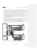
Add GND vias around transmission line, as described in
Formatted:
English (U.S.)
Formatted:
English (U.S.)
Formatted:
English (U.S.)
Formatted:
English (U.S.)
Formatted:
English (U.S.)
Formatted:
English (U.S.)
Formatted:
English (U.S.)
Formatted:
English (U.S.)