LILY-W1 series - System integration manual
UBX-15027600 - R09
Design-in
Page 25 of 64
C1 - Public
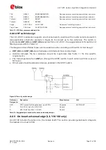
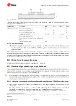
Figure 9: USB differential pair, controlled impedance parameters
The USB data lines must follow the recommendations stated in Table 16 to guarantee bus signal
integrity and avoid EMI issues.
Signal Group
Parameter
Min.
Typ.
Max.
Unit
USB differential data
Single Ended impedance,
𝑍𝑍
𝑆𝑆𝑆𝑆
45
Ω
Differential impedance,
𝑍𝑍
𝑑𝑑𝑖𝑖𝑑𝑑𝑑𝑑
90
Ω
Common mode impedance,
𝑍𝑍
𝐶𝐶𝐶𝐶
30
Ω
Impedance control,
𝑍𝑍
𝑆𝑆𝑆𝑆
,
𝑍𝑍
𝑑𝑑𝑖𝑖𝑑𝑑𝑑𝑑
,
𝑍𝑍
𝐶𝐶𝐶𝐶
𝑍𝑍
0
−
10%
𝑍𝑍
0
𝑍𝑍
0
+ 10%
Shunt capacitance to GND
5
pF
Bus skew length mismatch between differential
pair
0
15
mm
Isolation to other signals
4 w
Table 16: USB bus requirements
☞
USB data signals routed on the host board can have influence on the RF performance and
shunt capacitors or ESD protection filter to GND may be needed to reduce in-band noise from
USB harmonics.
If the USB data link is routed on a connector, the designer is encouraged to consider a common mode
choke and ESD protections on USB lines as options. Common mode chokes should be considered only
in case of EMI issues as they cause signal degradation. More details about proper selection of ESD
protections can be found in section 2.9.
2.5
Other interfaces and notes
All pins have internal keeper resistors; leave it open if not used.
2.6
General high speed layout guidelines
These general design guidelines are considered as best practices and are valid for any bus present in
the LILY-W1 modules. The designer should prioritize the layout of higher speed busses. Low
frequency signals are generally not critical for layout.
⚠
One exception is represented by High Impedance traces (such as signals driven by weak pull-
resistor) that may be affected by crosstalk. For those traces, a supplementary isolation of 4w from
other busses is recommended.
2.6.1
General considerations for schematic design and PCB floor-planning:
•
Verify which signal bus requires termination and add series resistor terminations to the
schematics.
•
Carefully consider the placement of the module with respect to antenna position and host
processor; RF trace length should be minimized first, followed by SDIO/USB bus length.
•
SDIO/USB bus routing should be planned to minimize layer-to-layer transition to a minimum.
10
Total mismatch includes skew introduced by cable and host side routing, keep it at minimum if USB bus is routed on a
connector.


