background image

© 2007 Funai Electric Co., Ltd.

All rights reserved. No part of this manual may be reproduced, copied, transmitted, disseminated, transcribed, 
downloaded or stored in any storage medium, in any form or for any purpose without the express prior written 
consent of Funai. Furthermore, any unauthorized commercial distribution of this manual or any revision hereto 
is strictly prohibited.  

Information in this document is subject to change without notice. Funai reserves the right to change the content 
herein without the obligation to notify any person or organization of such changes.  

 with the 

 design is a registered trademark of Funai Electric Co., Ltd and may not be used in any way 

without the express written consent of Funai. All other trademarks used herein remain the exclusive property of 
their respective owners. Nothing contained in this manual should be construed as granting, by implication or 
otherwise, any license or right to use any of the trademarks displayed herein. Misuse of any trademarks or any 
other content in this manual is strictly prohibited.  Funai shall aggressively enforce its intellectual property rights 
to the fullest extent of the law.

ZV450TT8

E9H11UD

2007-03-30

Содержание ZV450TT8

Страница 1: ...aration for Servicing I Adjustment Procedures I Schematic Diagrams I CBA s I Exploded Views I Parts List When servicing the deck mechanism refer to MK14 Deck Mechanism Section Deck Mechanism Part No N2460FL DVD RECORDER VIDEO CASSETTE RECORDER ZV450TT8 ...

Страница 2: ...mproper service methods may damage the equipment It also is important to understand that these CAUTIONS and NOTICES ARE NOT EXHAUSTIVE Funai could not possibly know evaluate and advice the service trade of all conceivable ways in which service might be done or of the possible hazardous consequences of each way Consequently Funai has not undertaken any such broad evaluation Accordingly a servicer w...

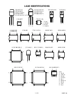
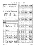
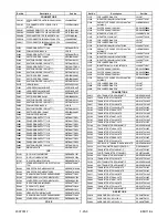
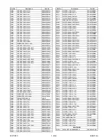
Страница 3: ...er VCR 1 8 1 Firmware Renewal Mode 1 9 1 Function Indicator Symbols 1 10 1 Block Diagrams 1 11 1 Schematic Diagrams CBA s and Test Points 1 12 1 Waveforms 1 13 1 Wiring Diagram VCR Section 1 14 1 Wiring Diagram DVD Section 1 14 2 System Control Timing Charts 1 15 1 IC Pin Function Descriptions 1 16 1 Lead Identifications 1 17 1 Exploded Views 1 18 1 Mechanical Parts List 1 19 1 Electrical Parts Li...

Страница 4: ...e W O Burst 1 4 Video Color S N AM R P dB 37 41 SP Mode 1 5 Video Color S N PM R P dB 30 36 SP Mode 1 6 Resolution PB Line 230 245 SP Mode 2 Servo 2 1 Jitter Low µsec 0 07 0 12 SP Mode 2 2 Wow Flutter 0 3 0 5 SP Mode 3 Normal Audio 3 1 Output PB dBV 9 6 3 SP Mode 3 2 Output R P dBV 9 6 1 5 SP Mode 3 3 S N R P dB 36 41 SP Mode 3 4 Distortion R P 1 0 4 0 SP Mode 3 5 Freq resp R P at 200Hz dB 11 4 SP...

Страница 5: ...omponent Output Y Luminance 75 ohm load Vp p 0 549 Cb Chrominance 75 ohm load Vp p 0 525 Cr Chrominance 75 ohm load Vp p 0 525 2 AUDIO 2 1 Output Level Vrms 2 0 2 2 Frequency Response DVD VIDEO LPCM fs 48kHz 20 22kHz dB 0 5 Audio CD fs 44 1kHz 20 20 kHz dB 0 5 2 3 Signal Noise Ratio DVD VIDEO LPCM dB 90 CD dB 90 REC Playback Input 2 Vrms Rec Speed XP dB 80 2 4 Dynamic Range DVD VIDEO LPCM dB 80 CD...

Страница 6: ...way from the pickup lens when the diode is turned on Do not look directly at the laser beam CAUTION Use of controls and adjustments or doing procedures other than those specified herein may result in hazardous radiation exposure Location Inside Top of DVD mechanism Do not look directly at the laser beam coming from the pickup or allow it to strike against your skin Drive Mechanism Assembly Laser B...

Страница 7: ...ical for safety Replace only with part number specified B In addition to safety other parts and assemblies are specified for conformance with regulations applying to spurious radiation These must also be replaced only with specified replacements Examples RF converters RF cables noise blocking capacitors and noise blocking filters etc C Use specified internal wiring Note especially 1 Wires covered ...

Страница 8: ...ug prongs and externally exposed accessible parts RF terminals antenna terminals video and audio input and output terminals microphone jacks earphone jacks etc is lower than or equal to the specified value in the table below Measuring Method Power ON Insert load Z between B earth ground power cord plug prongs and exposed accessible parts Use an AC voltmeter to measure across the terminals of load ...

Страница 9: ...machine then apply hot air to the Flat Pack IC about 5 to 6 seconds Fig S 1 1 2 Remove the flat pack IC with tweezers while applying the hot air 3 Bottom of the flat pack IC is fixed with glue to the CBA when removing entire flat pack IC first apply soldering iron to center of the flat pack IC and heat up Then remove glue will be melted Fig S 1 6 4 Release the flat pack IC from the CBA using tweez...

Страница 10: ... by one using a sharp pin or wire to which solder will not adhere iron wire When heating the pins use a fine tip soldering iron or a hot air desoldering machine Fig S 1 4 3 Bottom of the flat pack IC is fixed with glue to the CBA when removing entire flat pack IC first apply soldering iron to center of the flat pack IC and heat up Then remove glue will be melted Fig S 1 6 4 Release the flat pack I...

Страница 11: ...rs Fig S 1 6 Note When using a soldering iron care must be taken to ensure that the flat pack IC is not being held by glue When the flat pack IC is removed from the CBA handle it gently because it may be damaged if force is applied 2 Installation 1 Using desoldering braid remove the solder from the foil of each pin of the flat pack IC on the CBA so you can install a replacement flat pack IC more e...

Страница 12: ...ed to remove any static electricity that may be charged on the body 2 Ground for Workbench Be sure to place a conductive sheet or copper plate with proper grounding 1 MΩ on the workbench or other surface where the semi conductors are to be placed Because the static electricity charge on clothing will not escape through the body grounding band be careful to avoid contacting semi conductors with you...

Страница 13: ...nto the Deck Mechanism Assembly and press the PLAY button The tape will be loaded into the Deck Mechanism Assembly Make sure the power is on connect TP502 S INH to GND This will stop the function of Tape Start Sensor Tape End Sensor and Reel Sensors If these TPs are connected before plugging in the unit the function of the sensors will stay valid See Fig 1 Note Because the Tape End Sensors are ina...

Страница 14: ...Bracket 4 Jack Bracket 5 Front Jack CBA 6 DVD Mechanism DVD Main CBA Assembly 8 Rear Panel Unit 15 Power Supply CBA 12 DC Fan Motor 9 Tuner CBA 16 PCB Holder 13 D T Bracket R 10 DTV Module CBA Unit 19 Deck Assembly 23 Deck Pedestal 21 DVD Open Close SW CBA 18 VCR Chassis Unit 17 D T Bracket L 20 Power SW CBA 22 Main CBA 24 Front Bracket R 11 Fan Holder 7 Dust Cover D4 8 Rear Panel Unit D5 6 S 6 3 ...

Страница 15: ...cking Tabs L 1 1 2 Release three Locking Tabs L 2 1 3 Disconnect Connector CN1609 and remove the Front Assembly 2 When reassembling solder wire jumpers as shown in Fig D8 3 Before installing the Deck Assembly be sure to place the pin of LD SW on Main CBA as shown in Fig D8 Then install the Deck Assembly while aligning the hole of Cam Gear with the pin of LD SW the shaft of Cam Gear with the hole o...

Страница 16: ...CN701 S 5 6 DVD Mechanism DVD Main CBA Assembly 7 Dust Cover Fig D5 S 6 S 7 S 7 S 7 CN1102 CN2610 CN2611 S 9 S 9 8 Rear Panel Unit S 8 9 Tuner CBA 10 DTV Module CBA UNIT Fig D6 S 10 S 11 14 Rear Panel 13 D T Bracket R 12 DC Fan Motor 11 Fan Holder ...

Страница 17: ...1 6 4 E9H11DC CN1101 Fig D7 S 13 S 12 S 12 15 Power Supply CBA 16 PCB Holder Fig D8 S 15 S 15 S 15 S 16a S 17 S 18 S 14 S 16a S 16a S 16b 18 VCR Chassis Unit 17 D T Bracket L ...

Страница 18: ...th blue stripe 22 Main CBA SW1512 LD SW From FE Head BOTTOM VIEW Lead connections of Deck Assembly and Main CBA Desolder From Capstan Motor Assembly Printing side Desolder From Cylinder Assembly From ACE Head Assembly Lead with blue stripe Lead with blue stripe Desolder Lead with gray stripe S 19 S 20 Fig D9 LD SW Pin Hole Hole Shaft Cam Gear 22 Main CBA 19 Deck Assembly Pin ...

Страница 19: ...1 6 6 E9H11DC Fig D10 23 Deck Pedestal 24 Front Bracket R S 21 S 21 S 21 S 21 S 22 ...

Страница 20: ... the Front Bracket 4 Remove the DVD Mechanism DVD Main CBA Assembly 5 Unhook two places and detach the Dust Cover 6 Rotate the gear in the direction of the arrow manually as shown below until the tray descends 7 Pull the tray out manually and remove a disc View for A Rotate this gear in the direction of the arrow hook Front Bracket Front Assembly Dust Cover A ...

Страница 21: ... 001 50 V Div F Range DC AC 20 MHz 2 Alignment Tape FL8A Head Switching Position Adjustment Purpose To determine the Head Switching position during playback Symptom of Misadjustment May cause Head Switching noise or vertical jitter in the picture Note TP751 V OUT TP302 RF SW VR1501 Switching Point Main CBA Reference Notes Playback the Alignment tape and adjust VR501 so that the V sync front edge o...

Страница 22: ...alizing is completed the DVD recorder exits the Version display mode and turns off the power automatically To move into the Normal mode from the Version display mode press RETURN button on the remote control instead of ENTER button When POWER button is pressed before ENTER button is pressed the DVD recorder exits the Version display mode then the power turns off MODEL NAME DTV S VERSION FE VERSION...

Страница 23: ...own in 1 of Fig d is described as follows 5 After updating is finished the tray opens automatically At this time no button is available 6 Pull out the AC code once then insert it again Fig a Version Up Mode Screen Firmware Version differs depending on the models and this indication is one example Current F W version is displayed Firm Update Mode Please insert a disc ver WD4F S1E Fig b VFD in Versi...

Страница 24: ...orking properly P ON 5V Power safety detection Led Mode Indicator Active When reel or capstan mechanism is not functioning correctly A R is displayed on a TV screen Refer to Fig 1 When tape loading mechanism is not functioning correctly A T is displayed on a TV screen Refer to Fig 2 When cassette loading mechanism is not functioning correctly A C is displayed on a TV screen Refer to Fig 3 When the...

Страница 25: ...utes 12 Difference in the address and can not get StreamID of RDI VIDEO 13 It is a reply that ATAPI is not readable 14 Cannot write the data after recovering SMALL VMGI 15 Cannot write the data after DVD R Reverse Track 16 An error occurs in Finalize Close 17 An error occurs in Rec Stop Close 18 An error occurs in PCA Full DVD_R 19 Safety Stop occurs during editing 20 High Speed Disc 2 21 The disc...

Страница 26: ...rs 33 The 999 chapter has been reached VR Format Disc 9 You cannot record on this disc as Control Information is full Delete unnecessary titles 34 There is not space to record field of control information 10 You cannot record on this disc as Power Calibration Area is full Insert a new disc 35 PCA is Full in REC start 4 This disc is already finalized Release the finalizing for this disc 36 It is fi...

Страница 27: ...tart time Insert a recordable videotape with a record tab 40 Some portion has not been recorded because of program overlapping Recording did not start at the start time No Videotape is inserted Videotape ran out during recording Turn the power on and set the clock correctly then set timer programming again 41 Power failed Insert the recordable disc 42 No disc when recording ...

Страница 28: ... BLOCK DIAGRAM TO POWER SUPPLY BLOCK DIAGRAM IIC BUS SDA IIC BUS SCL 17 18 IIC BUS SCL IIC BUS SDA NORMAL L 78 Hi Fi H SW Hi Fi NOR IN Hi Fi H SW 30 OUTPUT SELECT OUTPUT SELECT DISPLAY DATA 7 DISPLAY CLK CLK 1G 2G 4G 5G 6G 7G a b c d e f h i g 3G GRID SEGMENT VFD STB DIN 8 REMOTE 5 REMOTE SENSOR RS1501 FL1501 2 28 1 21 22 23 18 17 19 20 9 8 7 12 13 14 16 11 10 60 61 AUDIO SW1 AUDIO SW2 AUDIO SW1 A...

Страница 29: ... 34 DECK ASSEMBLY END S T REEL T REEL ST S ST S Q1504 Q1503 Q1506 SW POINT AL 5V VR1501 TP506 TP505 END S TP507 SW1511 REC SW LD SW 87 AL 12V AL 5V AL 5V SW1512 AL 18V P ON 5V 1 MODE SW AL 5V D1555 S LED 5 CTL 6 CTL 1 AL 12V 1 2 P ON 5V 1 3 C FG 4 C F R 5 C CONT 6 GND 7 LM FWD REV 8 D CONT 9 D PFG 10 GND 11 AL 12V 12 AL 18V TP513 CTL AL 12V 1 MAIN CBA CAPSTAN MOTOR CYLINDER ASSEMBLY DRUM MOTOR PG ...

Страница 30: ...1 DVD MECHANISM TILT TRACKING FOCUS PICK UP SLED MOTOR M REC VIDEO SIGNAL PB VIDEO SIGNAL REC AUDIO SIGNAL PB AUDIO SIGNAL LPC LPC MAIN MICRO CONTROLLER CN1001 SPINDLE MOTOR M CN1002 RELAY CBA CN301 3 3V VIDEO Y CVBS VIDEO C IC701 VIDEO DECODER DECODER A D 45 50 U4 W1 W3 Y2 AA1 AA2 DECODER A D 39 44 P3 T3 T5 U2 U3 V1 10 8 13 M5 VIDEO Y I D A SPDIF DVD AUDIO MUTE DVD AUDIO MUTE AUDIO L OUT AUDIO R ...

Страница 31: ... DIAGRAM TO VIDEO OUTPUT SELECT BLOCK DIAGRAM VCR VIDEO DVD VIDEO DUB VCR DVD TO SYSTEM CONTROL BLOCK DIAGRAM CYLINDER ASSEMBLY RF SW RF SW 59 V ENV H A SW H A COMP H A COMP TP302 VIDEO L 2 HEAD VIDEO R 2 HEAD TP301 C PB D V SYNC C SYNC D V SYNC 25 53 24 YCA SCL 14 36 37 39 34 Q1301 BUFFER 30 58 60 SP EP 54 YCA SDA 55 YCA CS SERIAL I F VCA CLAMP 69 70 SP HEAD AMP EP HEAD AMP 72 73 74 65 66 67 ENV ...

Страница 32: ... 23 24 VIDEO SW2 TO SYSTEM CONTROL BLOCK DIAGRAM VIDEO SW3 FRONT JACK CBA CONTROL LOGIC PB EE BUFFER BUFFER BUFFER LPF LPF DVD MAIN CBA UNIT CN701 20 20 VIDEO Y CVBS IN 22 22 VIDEO C IN CN2201 VCR VIDEO TO VIDEO BLOCK DIAGRAM Q2304 BUFFER Q2305 BUFFER VCR VIDEO DUB TO VIDEO BLOCK DIAGRAM VIDEO SW1 VCR DVD DUBBING 20 VIDEO Y CVBS VIDEO C IC5002 INPUT SELECT SW CTL DTV VIDEO TO SYSTEM CONTROL BLOCK ...

Страница 33: ...dB AMP LPF DRIVER 6 10 4dB AMP 2dB AMP LPF DRIVER 8 VIDEO Pb Cb OUT VIDEO Y OUT VIDEO Pr Cr OUT JK2403 REAR VIDEO OUT COMPOSITE JK2751 REAR TP751 V OUT 3 TO DIGITAL SIGNAL PROCESS BLOCK DIAGRAM DVD VIDEO DUB SW CTL PB EE VIDEO TO VIDEO BLOCK DIAGRAM REC VIDEO SIGNAL PB VIDEO SIGNAL WF4 WF5 WF6 WF1 WF7 WF8 15 10 9 11 OUTPUT SELECT Q2391 BUFFER DVD VCR DUBBING IC2404 VIDEO DRIVER 5 4dB AMP 2dB AMP L...

Страница 34: ...R ALC AUDIO PROCESS 76 80 78 TUNER LINE 1 LINE 2 4 AUDIO PB REC CN1504 3 A COM 1 AE H 2 AE H FE H AUDIO HEAD AUDIO ERASE HEAD AC HEAD ASSEMBLY FE HEAD DECK ASSEMBLY 1 FE H 2 FE H GND CN1501 MAIN CBA PB AUDIO SIGNAL REC AUDIO SIGNAL 58 55 53 54 D REC AUDIO MUTE TO SYSTEM CONTROL BLOCK DIAGRAM FULL ERASE HEAD YCA CS YCA SCL YCA SDA IC1301 N A OUT N A IN TO Hi Fi AUDIO BLOCK DIAGRAM 3 2 4 5 ...

Страница 35: ...AUDIO R OUT2 TO SYSTEM CONTROL BLOCK DIAGRAM TO Hi Fi AUDIO BLOCK DIAGRAM CN2609 CN2605 REC AUDIO SIGNAL PB AUDIO SIGNAL 12 13 5 3 14 4 DVD PB DVD VCR DUBBING TP754 A OUT L TP753 A OUT R WF10 WF9 9 10 11 DVD MAIN CBA UNIT 3 3 SPDIF 17 17 AUDIO L OUT 15 15 AUDIO R OUT 18 18 DVD AUDIO MUTE 11 11 AUDIO L IN 13 13 AUDIO R IN TO DIGITAL SIGNAL PROCESS BLOCK DIAGRAM IC802 AUDIO A D CONVERTER AUDIO A D C...

Страница 36: ...IM 49 LINE L OUT LINE R OUT N A IN Hi Fi H SW AUDIO MUTE NORMAL L TO AUDIO BLOCK DIAGRAM IIC BUS SDA IIC BUS SCL P ON 9V TO SYSTEM CONTROL BLOCK DIAGRAM MAIN CBA Hi Fi AUDIO R 7 Hi Fi COM 8 Hi Fi AUDIO L 9 CN1253 IC1451 MTS SAP Hi Fi AUDIO PROCESS Hi Fi HEAD AMP REC AUDIO SIGNAL PB AUDIO SIGNAL Mode SP REC TO AUDIO BLOCK DIAGRAM TO SYSTEM CONTROL BLOCK DIAGRAM TO SYSTEM CONTROL BLOCK DIAGRAM DVD A...

Страница 37: ...1105 Q1057 SW 5V 3 3V REG IC2503 2 5V REG IC2504 P ON 2 5V P ON 2 5V Q1107 Q1108 FAN CONTROL REG CONT1 REG CONT2 SWITCHING Q2205 SWITCHING Q2206 Q5001 4 5 8 17 19 20 25 29 30 6 7 18 26 27 28 2 5V REG IC5004 SWITCHING CAUTION Fixed voltage or Auto voltage selectable power supply circuit is used in this unit If Main Fuse F1001 is blown check to see that all components in the power supply circuit are...

Страница 38: ... X281 4 5 VIDEO ENCODER AUDIO DECODER AUDIO D A CONVERTER 14 14 SDA 15 15 SCL 14 15 CN5005 L CH R CH SDA SCL TO VIDEO INPUT SELECT BLOCK DIAGRAM TO AUDIO INPUT OUTPUT SELECT BLOCK DIAGRAM TO SYSTEM CONTROL BLOCK DIAGRAM CN5005 CN101 DTV VIDEO DTV AUDIO L DTV AUDIO R CN102 WF11 WF12 IC202 FLASH MEMORY DTV MODULE CBA UNIT SDRAM I F FLASH MEMORY I F IC201 DDR SDRAM 1 1 79 81 85 87 89 91 92 94 96 98 1...

Страница 39: ...k in the schematic diagram and the parts list Before replacing any of these components read the parts list in this manual carefully The use of substitute replacement parts that do not have the same safety characteristics as specified in the parts list may create shock fire or other hazards Notes 1 Do not use the part number shown on these drawings for ordering The correct part number is shown in t...

Страница 40: ...y original replacement parts which are listed with their part numbers in the parts list section of the service manual 4 Mode SP REC 5 Voltage indications for PLAY and REC modes on the schematics are as shown below 6 How to read converged lines 7 Test Point Information A V F This symbol means fast operating fuse Ce symbole represente un fusible a fusion rapide 2 3 1 5 0 2 5 PLAY mode STOP mode 5 0 ...

Страница 41: ...1 12 3 Main 1 8 Schematic Diagram E9H11SCM1 ...

Страница 42: ...11SCM2 PM DTV BS CS CD VCR HDD DVD DR DB T C 5G 4G 3G 2G 1G 7G 6G a b c d e f g 7G 6G 5G 4G 3G 2G 1G P1 P2 P3 P4 P5 P6 P7 d P8 S1 P9 f g c e a b d f g c e a b d f g c e a b d f g c e a b d f g c e a b d f g c e a b FL1501 MATRIX CHART PM BS CS DR CD VCR DB HDD DVD DTV T C ...

Страница 43: ...1 12 5 Main 3 8 Schematic Diagram E9H11SCM3 ...

Страница 44: ...1 12 6 Main 4 8 Schematic Diagram E9H11SCM4 ...

Страница 45: ...1 12 7 Main 5 8 Schematic Diagram E9H11SCM5 ...

Страница 46: ...1 12 8 Main 6 8 Schematic Diagram E9H11SCM6 ...

Страница 47: ...1 12 9 Main 7 8 Schematic Diagram E9H11SCM7 ...

Страница 48: ...1 12 10 Main 8 8 Schematic Diagram E9H11SCM8 ...

Страница 49: ...er supply Otherwise it may cause some components in the power supply circuit to fail Ce symbole reprèsente un fusible à fusion rapide CAUTION For continued protection against fire hazard replace only with the same type fuse ATTENTION Pour une protection continue les risqes d Incele n utiliser que des fusible de même type Risk of fire replace fuse as marked This symbol means fast operating fuse A V...

Страница 50: ...1 12 12 Front Jack Schematic Diagram E9H11SCFJ ...

Страница 51: ...005 1 0 2 1 6 3 5 1 4 3 4 5 3 2 6 0 7 3 0 8 3 3 9 3 2 10 0 8 11 0 12 3 3 13 0 14 3 1 15 3 1 16 0 2 17 5 0 18 0 19 3 4 20 2 6 21 1 8 22 3 4 23 0 24 3 0 25 0 26 0 27 0 28 0 29 0 4 30 2 5 31 2 5 32 0 33 1 0 34 0 4 35 0 1 VOLTAGE CHART Pin No Voltage ...

Страница 52: ... 5 Schematic Diagram E9H11SCD1 The order of pins shown in this diagram is different from that of actual IC101 IC101 is divided into five and shown as IC101 1 5 IC101 5 5 in this DVD Main Schematic Diagram Section 1 NOTE ...

Страница 53: ... 5 Schematic Diagram E9H11SCD2 The order of pins shown in this diagram is different from that of actual IC101 IC101 is divided into five and shown as IC101 1 5 IC101 5 5 in this DVD Main Schematic Diagram Section 1 NOTE ...

Страница 54: ... 5 Schematic Diagram E9H11SCD3 The order of pins shown in this diagram is different from that of actual IC101 IC101 is divided into five and shown as IC101 1 5 IC101 5 5 in this DVD Main Schematic Diagram Section 1 NOTE ...

Страница 55: ...DVD Main 4 5 Schematic Diagram The order of pins shown in this diagram is different from that of actual IC101 IC101 is divided into five and shown as IC101 1 5 IC101 5 5 in this DVD Main Schematic Diagram Section 1 NOTE ...

Страница 56: ... 5 Schematic Diagram E9H11SCD5 The order of pins shown in this diagram is different from that of actual IC101 IC101 is divided into five and shown as IC101 1 5 IC101 5 5 in this DVD Main Schematic Diagram Section 1 NOTE ...

Страница 57: ...1 12 19 DTV Module 1 2 Schematic Diagram E9H11SCDTV1 ...

Страница 58: ...1 12 20 DTV Module 2 2 Schematic Diagram E9H11SCDTV2 ...

Страница 59: ...1 12 21 SW POINT VR1501 CTL TP513 RF SW TP302 WF2 C PB TP301 WF3 V OUT TP751 WF1 S INH TP502 BE9E8AF01011A Main CBA Top View Sensor CBA Top View BHF300F01012A BHF300F01012B ...

Страница 60: ...1 12 22 PIN 2 OF IC2406 WF6 PIN 5 OF CN2201 WF8 PIN 3 OF CN2201 WF7 PIN 17 OF CN2201 WF9 PIN 9 OF CN2201 WF5 PIN 7 OF CN2201 WF4 PIN 3 OF CN2204 WF10 Main CBA Bottom View BE9E8AF01011A ...

Страница 61: ...ply circut an isolation transformer must be used Also in order to have the ability to increase the input slowly when troubleshooting this type power supply circuit a variable isolation transformer is required CAUTION Fixed voltage or Auto voltage selectable power supply circuit is used in this unit If Main Fuse F1001 is blown check to see that all components in the power supply circuit are not def...

Страница 62: ...pply circut an isolation transformer must be used Also in order to have the ability to increase the input slowly when troubleshooting this type power supply circuit a variable isolation transformer is required CAUTION Fixed voltage or Auto voltage selectable power supply circuit is used in this unit If Main Fuse F1001 is blown check to see that all components in the power supply circuit are not de...

Страница 63: ...1 12 25 BE9C80F01032A Tuner CBA Top View ...

Страница 64: ...1 12 26 PIN 14 OF TU5001 PIN 15 OF TU5001 WF11 WF12 PIN 4 OF TU5001 WF13 Tuner CBA Bottom View BE9C80F01032A ...

Страница 65: ...27 Front Jack CBA Top View Front Jack CBA Bottom View Power SW CBA Top View Power SW CBA Bottom View BE9E8AF01021B BE9E8AF01011C BE9E8AF01011B DVD Open Close SW CBA Top View DVD Open Close SW CBA Bottom View ...

Страница 66: ... Pin 9 of CN2201 VIDEO C 0 2V 20µs WF6 Pin 2 of IC2406 VIDEO CVBS 0 5V 20µs NOTE Input COLOR BAR SIGNAL WITH 1KHz AUDIO SIGNAL WF3 WF1 UPPER WF2 WF2 LOWER TP751 TP302 UPPER LOWER TP302 TP301 V OUT 0 5V 50µs RF SW 5V C PB RF SW 5V 5ms 0 2V WF1 TP751 V OUT E E 0 2V 20µs WF11 Pin 14 of TU5001 PLL CLK 2V 2ms WF12 Pin 15 of TU5001 PLL DATA 2V 2ms WF13 Pin 4 of TU5001 TU AUDIO 0 5V 0 2ms TU VIDEO 0 2V 2...

Страница 67: ...Y 29 SUB RXD 30 SYS RESET 27 SPDIF 3 GND 2 EV 10 5V 27 EV 10 5V 26 EV 10 5V 25 GND 24 GND 23 GND 19 GND 18 P ON 5V 22 P ON 5V 21 P ON 5V 20 EV 2 4V 12 EV 2 4V 11 EV 2 4V 10 GND 14 GND 13 1V2CONT 1 GND 8 P ON 2 5V 7 P ON 2 5V 6 GND 9 GND 5 GND 4 P ON 3 3V 17 P ON 3 3V 16 P ON 3 3V 15 GND 28 GND 29 GND 30 POWER SUPPLY CBA AC CORD DTV MODULE CBA UNIT TUNER CBA CN102 CN5005 GND 1 1 TUNER 5V 3 3 NU 4 4...

Страница 68: ...P ON 5V 20 EV 2 4V 12 EV 2 4V 11 EV 2 4V 10 GND 14 GND 13 1V2CONT 1 GND 8 P ON 2 5V 7 P ON 2 5V 6 GND 9 GND 5 GND 4 P ON 3 3V 17 P ON 3 3V 16 P ON 3 3V 15 GND 28 GND 29 GND 30 DVD MAIN CBA UNIT DVD MECHANISM PICKUP RELAY CBA CN201 CN1001 10 9 HW 9 10 HW 1 FCS 4 TRK 3 TRK 2 FCS 6 TILT 5 TILT 7 LDD IIN4 9 LDD IIN2 10 LDD IINR 11 NU 8 LDD IIN3 12 LDD VDD 14 LDD ENABLE 15 LDD OSCEN 16 GND 17 LDD WEN4 ...

Страница 69: ... CHARTS INNER SW open INNER SW open To disc distinction Power on Yes Yes No No Tray insertion Tray insertion Tray Open button is pressed Tray Open button is pressed Tray ejection Tray ejection SLED moves Push Close INNER SW open Yes No ...

Страница 70: ...5 V T2 2 000 s V2 2 00 V T3 0 008 s V3 2 36 V T4 0 006 s V4 4 26 V T5 0 066 s T6 1 500 s T7 0 800 s T8 0 005 s SLED INNER SW close open Tray insertion direction Tray ejection direction T4 T2 T5 V0 V2 V1 T3 T1 SLED INNER SW close open Tray insertion direction Tray ejection direction V3 V4 T6 T7 T8 ...

Страница 71: ...1 15 3 R4NTI Push close 0 08 V 0 02 s Push Close detection Threshold level ...

Страница 72: ...Safety SW Detect With Record tab L Without Record tab H 23 OUT RF SW Video Head Switching Pulse 24 OUT D V SYNC Dummy V sync Output 25 IN RESET System Reset Signal Reset L 26 OUT LM FWD REV Loading Motor FWD REV Output 27 OUT P ON L Power On Signal to Low 28 NU Not Used 29 OUT D REC Delayed Record Signal 30 OUT Hi Fi H SW Hi Fi Audio Head Switching Pulse 31 OUT VCR AUDIO MUTE VCR Audio Mute Contro...

Страница 73: ... Signal 78 IN Hi Fi NOR IN Audio Mode Input HiFi L Normal H 79 IN DVD POWER SAFETY DVD Power Supply Safety Signal 80 IN VCR POWER SAFETY VCR Power Supply Safety Signal Pin No IN OUT Signal Name Function 81 IN END S Tape End Position Detect Signal 82 IN AFC Automatic Frequency Control Signal 83 IN V ENV Video Envelope Comparator Signal 84 IN PG DELAY Video Head Switching Pulse Signal Adjusted Volta...

Страница 74: ...trobe 3 NU Not Used 4 NU Not Used 5 VSS Ground 6 VDD Power Supply 7 OUT a Segment Output 8 b 9 c 10 d 11 e 12 f 13 g 14 h 15 VEE Pull Down Level 16 OUT i Segment Output 17 OUT 7G Grid Output 18 6G 19 5G 20 4G 21 3G 22 2G 23 1G 24 VDD Power Supply 25 VSS Ground 26 IN OSC Oscillator Input 27 NU Not Used 28 IN DIN Serial Data Input ...

Страница 75: ... 24 13 1 4 8 5 KRA103M AT P KRC103M AT P KTA1267 GR AT P KTC3193 Y AT P KTC3199 BL GR Y AT P KTA 1266 GR AT P KTC3198 GR AT P KTC3203 Y AT P KTC3266 GR AT P LA71205M MPB E Note A Anode K Cathode E Emitter C Collector B Base R Reference S Source G Gate D Drain PS2561A 1 W PT204 6B 12 MM1636XWRE CD4052BNSR CD4053BNSR RN1511 TE85R F PQ070XF01SZH 2SK3563 Q MM1637XVBE MM1697AJBE AN5832SA E1V LA72670BM ...

Страница 76: ...13 2L054 DVD Open Close SW CBA 2L030 2L033 2B17 2B14 1B1 2L017 2L017 2L017 2B1 2L021 2L022 2B16 2L033 2L071 2L011 2B2 2B31 Power SW CBA 2L045 2L052 2L045 A18 A1X 1B2 2B76 2B10 2B4 2B3 2L043 2L044 2L019 2L111 2L111 2L033 2L068 2L082 2L081 2L062 2L069 2L081 2L075 2L075 2L068 2L011 2L011 A2 2B86 2L081 Sensor CBA AC1001 DVD Mechanism DVD Main CBA Assembly Main CBA Power Supply CBA RS1501 2L068 Tuner A...

Страница 77: ...1 18 2 E9H11PEX Packing S1 A14 S2 Unit S3 Some Ref Numbers are not in sequence X1 X22 X4 X20 X5 X2 X3 S2 ...

Страница 78: ...HEAD GBCC3050 2L013 SCREW S TIGHT M3X6 BIND HEAD GBJS3060 2L014 SCREW S TIGHT M3X6 BIND HEAD GBJS3060 2L017 SCREW S TIGHT M3X8 BIND HEAD GBJS3080 2L021 SCREW P TIGHT M3X8 BIND HEAD GBCP3080 2L022 SCREW S TIGHT M3X6 BIND HEAD GBJS3060 2L030 SCREW P TIGHT M3X8 BIND HEAD GBJP3080 2L033 SCREW S TIGHT M3X6 BIND HEAD GBJS3060 2L043 SCREW P TIGHT M3X8 BIND HEAD GBJP3080 2L044 SCREW S TIGHT M3X8 BIND HEAD...

Страница 79: ...AP 1608 B K 0 01µF 50V CHD1JK30B103 C1330 ELECTROLYTIC CAP 1µF 50V M H7 CE1JMAVSL1R0 C1331 CHIP CERAMIC CAP 1608 B K 0 01µF 50V CHD1JK30B103 C1332 ELECTROLYTIC CAP 1µF 50V M H7 CE1JMAVSL1R0 C1333 CHIP CERAMIC CAP 1608 F Z 0 1µF 50V CHD1JZ30F104 C1336 CHIP CERAMIC CAP 1608 B K 0 01µF 50V CHD1JK30B103 C1339 CHIP CERAMIC CAP 1608 B K 0 047µF 50V CHD1JK30B473 C1340 CHIP CERAMIC CAP 1608 B K 0 1µF 50V ...

Страница 80: ...1608 B K 0 1µF 50V CHD1JK30B104 C2403 ELECTROLYTIC CAP 1µF 50V M H7 CE1JMASSL1R0 C2423 CHIP CERAMIC CAP 1608 B K 0 01µF 50V CHD1JK30B103 C2441 ELECTROLYTIC CAP 1µF 50V M CE1JMASDL1R0 Ref No Description Part No C2442 ELECTROLYTIC CAP 470µF 6 3V M CE0KMASDL471 C2443 ELECTROLYTIC CAP 470µF 6 3V M CE0KMASDL471 C2461 ELECTROLYTIC CAP 1µF 50V M H7 CE1JMASSL1R0 C2462 ELECTROLYTIC CAP 470µF 6 3V M CE0KMAS...

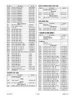
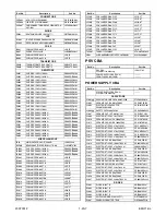
Страница 81: ...ZBA0TTY093 IC5004 VOLTAGE REGULATOR PQ070XF01SZH QSZBA0SSH054 COILS Ref No Description Part No L1251 PCB JUMPER D0 6 P5 0 JW5 0T L1303 INDUCTOR 100µH K LAP02TA101K LLAXKATTU101 L1304 RADIAL TYPE CHOKE COIL CW68 470K 841040NP LLBD00PKV023 L1305 CHIP RES 1608 1 10W 0 Ω RRXAJR5Z0000 L1306 CHIP RES 1608 1 10W 0 Ω RRXAJR5Z0000 L1421 INDUCTOR 47µH K 5FT LLARKBSTU470 L1422 INDUCTOR 22µH K 26T LLAXKATTU22...

Страница 82: ...457 CHIP RES 1 10W J 470 Ω RRXAJR5Z0471 R1458 CHIP RES 1 10W J 3 3k Ω RRXAJR5Z0332 Ref No Description Part No R1459 CHIP RES 1 10W J 39k Ω RRXAJR5Z0393 R1463 CHIP RES 1 10W J 39k Ω RRXAJR5Z0393 R1464 CHIP RES 1 10W J 12k Ω RRXAJR5Z0123 R1465 CHIP RES 1 10W J 47k Ω RRXAJR5Z0473 R1466 CHIP RES 1 10W J 6 8k Ω RRXAJR5Z0682 R1468 CHIP RES 1 10W J 470 Ω RRXAJR5Z0471 R1469 CHIP RES 1 10W J 1k Ω RRXAJR5Z0...

Страница 83: ... 1 10W J 75 Ω RRXAJR5Z0750 R2521 CHIP RES 1 10W J 2 2k Ω RRXAJR5Z0222 R2615 CHIP RES 1 10W J 1 2k Ω RRXAJR5Z0122 Ref No Description Part No R2616 CHIP RES 1 10W J 33k Ω RRXAJR5Z0333 R2617 CHIP RES 1 10W J 360 Ω RRXAJR5Z0361 R2751 CHIP RES 1 10W J 75 Ω RRXAJR5Z0750 R2771 CHIP RES 1608 1 10W 0 Ω RRXAJR5Z0000 R2772 CHIP RES 1608 1 10W 0 Ω RRXAJR5Z0000 R2777 CARBON RES 1 6W J 3 9k Ω RCX6JATZ0392 R2802...

Страница 84: ...A SST0101AL041 MISCELLANEOUS W101 WIRE ASSEMBLY 4P 4PIN AWG26 2651 P2 0 WX1E9A00 002 Ref No Description Part No Ref No Description Part No DVD OPEN CLOSE SW CBA MCV C Consists of the following SWITCHES SW1615 TACT SWITCH SKQSAF001A SST0101AL041 SW1617 TACT SWITCH SKQSAF001A SST0101AL041 MISCELLANEOUS W102 WIRE ASSEMBLY 3PIN 3PIN AWG26 2651 P2 0 WX1E9A00 003 Ref No Description Part No SENSOR CBA Co...

Страница 85: ...5018 PCB JUMPER D0 6 P6 0 JW6 0T JP5019 PCB JUMPER D0 6 P6 5 JW6 5T JP5020 PCB JUMPER D0 6 P5 0 JW5 0T Ref No Description Part No JP5022 PCB JUMPER D0 6 P12 5 JW12 5T JP5023 PCB JUMPER D0 6 P15 0 JW15 0T JP5025 PCB JUMPER D0 6 P20 0 JW20 0T JP5026 PCB JUMPER D0 6 P17 5 JW17 5T JP5027 PCB JUMPER D0 6 P11 5 JW11 5T JP5028 PCB JUMPER D0 6 P7 5 JW7 5T JP5029 PCB JUMPER D0 6 P17 5 JW17 5T JP5030 PCB JU...

Страница 86: ...9 CARBON RES 1 6W J 22k Ω RCX6JATZ0223 R1015 CARBON RES 1 4W J 820 Ω RCX4JATZ0821 R1016 CARBON RES 1 6W J 330 Ω RCX6JATZ0331 R1017 PCB JUMPER D0 6 P5 0 JW5 0T R1018 CARBON RES 1 6W J 4 7k Ω RCX6JATZ0472 R1019 CARBON RES 1 6W J 1 8k Ω RCX6JATZ0182 R1020 PCB JUMPER D0 6 P5 0 JW5 0T R1021 CARBON RES 1 6W G 2 4k Ω RCX6GATZ0242 R1022 CARBON RES 1 6W G 5 6k Ω RCX6GATZ0562 R1029 CARBON RES 1 6W J 150k Ω ...

Страница 87: ...herein without the obligation to notify any person or organization of such changes with the design is a registered trademark of Funai Electric Co Ltd and may not be used in any way without the express written consent of Funai All other trademarks used herein remain the exclusive property of their respective owners Nothing contained in this manual should be construed as granting by implication or o...

Отзывы: