background image

TE0600 TRM 

Revision: V3.02 

Copyright © 2017 Trenz Electronic GmbH

Page 

 of 

32

33

http://www.trenz-electronic.de

Disclaimer

Document Warranty

The material contained in this document is provided “as is” and is subject to being changed at any time 

without notice. Trenz Electronic does not warrant the accuracy and completeness of the materials in this 

document. Further, to the maximum extent permitted by applicable law, Trenz Electronic disclaims all 

warranties, either express or implied, with regard to this document and any information contained herein, 

including but not limited to the implied warranties of merchantability, fitness for a particular purpose or non 

infringement of intellectual property. Trenz Electronic shall not be liable for errors or for incidental or 

consequential damages in connection with the furnishing, use, or performance of this document or of any 

information contained herein.

Limitation of Liability

In no event will Trenz Electronic, its suppliers, or other third parties mentioned in this document be liable for 

any damages whatsoever (including, without limitation, those resulting from lost profits, lost data or business 

interruption) arising out of the use, inability to use, or the results of use of this document, any documents 

linked to this document, or the materials or information contained at any or all such documents. If your use 

of the materials or information from this document results in the need for servicing, repair or correction of 

equipment or data, you assume all costs thereof.

Copyright Notice

No part of this manual may be reproduced in any form or by any means (including electronic storage and 

retrieval or translation into a foreign language) without prior agreement and written consent from Trenz 

Electronic.

Technology Licenses

The hardware / firmware / software described in this document are furnished under a license and may be 

used /modified / copied only in accordance with the terms of such license.

Environmental Protection

To confront directly with the responsibility toward the environment, the global community and eventually 

also oneself. Such a resolution should be integral part not only of everybody's life. Also enterprises shall be 

conscious of their social responsibility and contribute to the preservation of our common living space. That 

is why Trenz Electronic invests in the protection of our Environment.

Содержание TE0600 TRM

Страница 1: ...TE0600 TRM Date Revision V3 02 03 Apr 2017 12 20...

Страница 2: ...________________________________________________ 12 Flash Memory ______________________________________________________________________ 13 Ethernet ____________________________________________________...

Страница 3: ...__________________ 30 Weight ____________________________________________________________________________ 30 Document Change History ______________________________________________________________ 31 D...

Страница 4: ...eading edge LX FPGA Gigabit Ethernet transceiver physical layer two Xilinx Spartan 6 independent banks of 16 bit wide 128 512 MBytes DDR3 SDRAM 16 MBytes SPI Flash memory for configuration and operati...

Страница 5: ...e through 1 kb protected 1 Wire EEPROM with SHA 1 Engine JTAG port SPI indirect FPGA configuration through B2B connector JTAG port SPI Flash memory Plug on module with 2 100 pin high speed hermaphrodi...

Страница 6: ...hly depend on the FPGA design implemented Some typical power consumptions are provided below for the following reference systems Boards GigaBee XC6SLX 45 100 150 Base board TE0603 02 Power supply 5 V...

Страница 7: ...m supply voltage is 3 0 volt The maximum supply voltage is 3 45 volt Warning Supply voltages beyond the range might affect to device reliability or even cause permanent damage of the device Board powe...

Страница 8: ...AM Power Rail memory chip By special request modules can be supplied without DDR3 SDRAM chips Contact Trenz Electronic support for details On board Power Rails GigaBee XC6SLX has the following power r...

Страница 9: ...5 V power rail if zero resistor R80 populated and R79 is is not from 1 5 V power rail if zero resistors R79 and R80 are populated and VCCIO0 connected to 1 5 V power not rail from an external power so...

Страница 10: ...to ensure proper system reset prior to a regular system start up The typical delay time td of 200 ms starts after the supply rail has risen above the threshold voltage After this delay the RESET line...

Страница 11: ...M connectors on the bottom side 2 x REF 189016 02 compatible to LSHM 150 04 0 L DV A S K TR 100 pins 50 per row 1 x REF 189017 02 compatible to LSHM 130 04 0 L DV A S K TR 60 pins 30 per row depending...

Страница 12: ...1 28 16 56 lshm_dv pdf 1 2013 11 28 16 56 tc0929 2611_qua 1 pdf 1 2013 11 28 16 55 EPROM GigaBee XC6SLX board contains a Maxim DS2502 E48 node address chip with factory programmed valid MAC 48 address...

Страница 13: ...ed to FPGA bank 2 and B2B connector J1 used pins are listed in the table below Flash signal FPGA pin J1 pin CS T5 87 CLK Y21 91 DI IO0 AB20 95 DO IO1 AA20 93 WP IO2 U14 99 HOLD IO3 U13 97 Serial flash...

Страница 14: ...g any user logic that is guaranteed to drive PHY reset low after FPGA configuration without using PHY clock Explanation Marvell PHY samples the MODE pins ONLY when it sees low level on PHY reset input...

Страница 15: ...he watchdog circuit within the time out interval min 1 1 s typ 1 6 s max 2 3 s the WDO watchdog output line becomes active low This event also re initializes the watchdog timer If zero resistors R2 is...

Страница 16: ...watchdog output line is left unconnected1 and the only possibility to reset the module is by driving the MR master reset line active low through pin 18 of connector J2 In the alternate assembly the W...

Страница 17: ...oard the JTAG interface can be accessed via connectors J5 and J6 on the carrier board Flash Configuration Default configuration option for FPGA is Master Serial SPI The bit stream for the FPGA is stor...

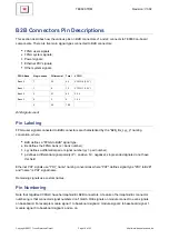
Страница 18: ...ors are characterized by the B2B_Bx_Lyy_p naming convention where B2B defines a FPGA to B2B signal type Bx defines the FPGA bank x bank number Lyy defines a differential pair or signal number yy pair...

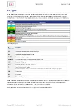
Страница 19: ...eral purpose user I O pin CONFIG Dedicated configuration signals PWRMGMT Control and status signals for the power saving Suspend mode JTAG Dedicated JTAG signals GND Dedicated ground pin All must be c...

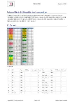
Страница 20: ...hould be soldered To provide connection B2B_B2_L41_N signal to AB13 FPGA pin zero resistor R81 should be soldered Note that in this case optional user oscillator U13 can t be used J1 Pin out J1 pin ou...

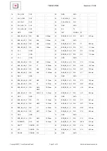
Страница 21: ...B2B_B2_L45_N DIO AB8 10 60mm 50 B2B_B2_L42_N DIO W11 7 52mm 51 B2B_B2_L45_P DIO AA8 11 053mm 52 B2B_B2_L42_P DIO V11 8 36mm 53 GND GND 54 GND GND 55 B2B_B2_L43_N DIO AB9 13 75mm 56 B2B_B2_L18_P DIO V1...

Страница 22: ..._N SIO Y12 13 58mm 93 MISO SPI AA20 94 B2B_B2_L10_N DIO R15 17 01mm 95 MOSI SPI AB20 96 B2B_B2_L10_P DIO R16 16 97mm 97 MISO3 SPI U13 98 B2B_B2_L2_N DIO AB21 5 06mm 99 MISO2 SPI U14 100 B2B_B2_L2_P DI...

Страница 23: ...9 28mm 43 B2B_B0_L7_P DIO D9 6 71mm 44 B2B_B0_L8_P DIO C9 9 92mm 45 B2B_B0_L33_N DIO C10 5 66mm 46 B2B_B0_L34_N DIO A10 7 58mm 47 B2B_B0_L33_P DIO D10 6 76mm 48 B2B_B0_L34_P DIO B10 8 60mm 49 GND GND...

Страница 24: ...B_B1_L59 SIO P19 27 19mm Signal Integrity Considerations Traces of differential signals pairs are routed symmetrically as symmetric pairs Traces of differential signals pairs are NOT routed with equal...

Страница 25: ...s Optimized placement and routing for DC DC converters Added thermal vias to mounting holes Added Testpoints Changed Board revision identification to REV03 Changed U9 from SIT1602AI 83 33E 25 0000 to...

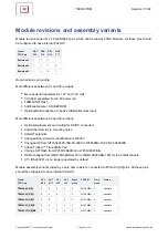
Страница 26: ...0 AV0 U19 Speed grade SDRAM Temp grade Status TE0600 03 V B 0 0 0 0 2 2x128MBit C full production TE0600 03 V B I 0 0 0 1 2 2x128MBit I full production TE0600 03 V B F 0 0 1 0 3 2x128MBit C full produ...

Страница 27: ...Winbond W25Q128BV product overview http www winbond com hq enu ProductAndSales ProductLines FlashMemory SerialFlash W25Q128BV htm Maxim DS2432 product page http www maximintegrated com datasheet index...

Страница 28: ...tp www xilinx com tools webpack htm http www xilinx com webpack Design Resources Trenz Electronic GigaBee Design Resources https shop trenz electronic de de Download path Trenz_Electronic TE0600 Trenz...

Страница 29: ...API application programming interface B2B board to board DSP digital signal processing digital signal processor EDK Embedded Development Kit IOB input output blocks I O blocks IP intellectual propert...

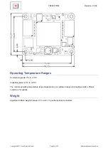
Страница 30: ...ronic de Operating Temperature Ranges Commercial grade 0 C to 70 C Industrial grade 40 C to 85 C The module operating temperature range depends also on customer design and cooling solution Please cont...

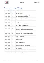
Страница 31: ...2 04 17 1 00 FDR Updated documentation link Replaced obsolete ElDesI and RedMine links with current GitHub links Updated dating convention 2012 05 18 1 01 AIK Corrected cross reference in section 3 2...

Страница 32: ...tation those resulting from lost profits lost data or business interruption arising out of the use inability to use or the results of use of this document any documents linked to this document or the...

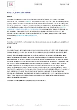
Страница 33: ...Directive 2002 96 EC of the European Parliament and of the Council of 27 January 2003 on waste electrical and electronic equipment WEEE Users of electrical and electronic equipment in private househol...

Отзывы: