Page 158
15. LCD Driver
15.2 Control
TMP86PM29BUG
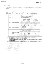
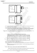
Note 1: When the TMP86PM29BUG uses the booster circuit to drive the LCD, the power supply and capacitor for the booster cir-
cuit should be connected as shown above.
Note 2: When the reference voltage is connected to a pin other than V1, add a capacitor between V1 and GND.
Note 3: The connection examples shown above are different from those shown in the datasheets of the previous version. Since
the above connection method enhances the boosting characteristics, it is recommended that new boards be designed
using the above connection method. (Using the existing connection method does not affect LCD display.)
Figure 15-3 Connection Examples When Using the Booster Circuit (LCDCR<BRES> = “1”)
Note 1: The current capacity is the amount of voltage that falls per 1
µ
A.
Note 2: The boosting frequency should be selected depending on your LCD panel.
Note 3: For the reference pin V1 or V2, a current capacity ten times larger than the above is recommended to ensure stable oper-
ation.
For example, when the boosting frequency is fc/2
9
(at fc = 8 MHz),
−
1.7 mV/
µ
A or more is recommended for the current
capacity of the reference pin V1.
15.2.3.2 When using an external resistor divider (LCDCR<BRES>="0")
When an external resistor divider is used, the voltage of an external power supply is divided and input
on V1, V2, and V3 to generate the output voltages for segment/common signals.
Table 15-3 V3 Pin Current Capacity and Boosting Frequency (typ.)
VFSEL
Boosting frequency
fc = 16 MHz
fc = 8 MHz
fc = 4 MHz
fc = 32.768 MHz
00
fc/2
13
or fs/2
5
−
37 mV/
µ
A
−
80 mV/
µ
A
−
138 mV/
µ
A
−
76 mV/
µ
A
01
fc/2
11
or fs/2
3
−
19 mV/
µ
A
−
24 mV/
µ
A
−
37 mV/
µ
A
−
23 mV/
µ
A
10
fc/2
10
or fs/2
2
−
17 mV/
µ
A
−
19 mV/
µ
A
−
24 mV/
µ
A
−
18 mV/
µ
A
11
fc/2
9
−
16 mV/
µ
A
−
17 mV/
µ
A
−
19 mV/
µ
A
–
V3
V2
V1
C1
C0
VDD
VSS
Keep the following
condition.
V3
C
C
C
C
= 0.1 to 0.47
µ
F
c) Reference pin = V3
C
Reference voltage
V3
V2
V1
C1
C0
VDD
VSS
Keep the following
condition.
C
C
C
C
= 0.1 to 0.47
µ
F
d) Reference pin = V3
C
V3 =
Содержание TLCS-870/C Series
Страница 1: ...8 Bit Microcontroller TLCS 870 C Series TMP86PM29BUG ...
Страница 6: ...TMP86PM29BUG ...
Страница 7: ...Revision History Date Revision 2007 10 11 1 First Release 2008 8 29 2 Contents Revised ...
Страница 9: ......
Страница 15: ...vi ...
Страница 19: ...Page 4 1 3 Block Diagram TMP86PM29BUG 1 3 Block Diagram Figure 1 2 Block Diagram ...
Страница 23: ...Page 8 1 4 Pin Names and Functions TMP86PM29BUG ...
Страница 48: ...Page 33 TMP86PM29BUG ...
Страница 49: ...Page 34 2 Operational Description 2 3 Reset Circuit TMP86PM29BUG ...
Страница 61: ...Page 46 3 Interrupt Control Circuit 3 8 External Interrupts TMP86PM29BUG ...
Страница 81: ...Page 66 6 Watchdog Timer WDT 6 3 Address Trap TMP86PM29BUG ...
Страница 135: ...Page 120 10 8 Bit TimerCounter TC5 TC6 10 1 Configuration TMP86PM29BUG ...
Страница 145: ...Page 130 11 Asynchronous Serial interface UART 11 9 Status Flag TMP86PM29BUG ...
Страница 165: ...Page 150 13 10 bit AD Converter ADC 13 6 Precautions about AD Converter TMP86PM29BUG ...
Страница 183: ...Page 168 15 LCD Driver 15 4 Control Method of LCD Driver TMP86PM29BUG ...
Страница 201: ...Page 186 18 Electrical Characteristics 18 9 Handling Precaution TMP86PM29BUG ...
Страница 203: ...Page 188 19 Package Dimensions TMP86PM29BUG ...
Страница 205: ......


