background image

3-36

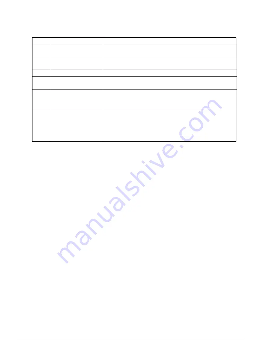
The contents of the HDC status register are described in Tables 3-4 and 3-5.

Bit

Name

Description

7

BBK

(Bad block mark)

"0"--Otherwise.
"1"--A bad block mark is detected.

6

UNC

(Uncorrectable)

"0"--There is no uncorrectable data error.
"1"--Uncorrectable data error has been detected.

5

Not used.

4

IDNF

(Identification)

"0"--Otherwise.
"1"--There was no ID field in the requested sector.

3

Not used.

2

ABRT

(Abort)

"0"--Otherwise.
"1"--Illegal command error or a drive status error occurs.

1

TK0

(Track 0)

"0"--The hard disk has found track 0 during a recalibrate
       command.
"1"--The hard disk could not find track 0 during a
       recalibrate command.

0

Not used.

Содержание T-Series T2000

Страница 1: ...1 1 Part 1 Hardware Overview ...

Страница 2: ...1 2 This page intentionally left blank ...

Страница 3: ...D specifications 1 10 Table 1 2 T2000 2 5 inch HDD specifications 1 11 Table 1 3 Sidelit LCD specifications 1 13 Table 1 4 FL inverter specifications 1 14 Figures Figure 1 1 T2000 personal computer 1 6 Figure 1 2 T2000 system unit configuration 1 6 Figure 1 3 T2000 block diagram 1 7 Figure 1 4 T2000 3 5 inch FDD 1 10 Figure 1 5 T2000 2 5 inch HDD 1 11 Figure 1 6 T2000 keyboard 1 12 Figure 1 7 Side...

Страница 4: ...1 4 This page intentionally left blank ...

Страница 5: ...ompatibility and 16 levels of gray The display controller supports VGA functions through the High Resolution Graphics Subsystem HRGS The 3 5 inch Floppy Disk Drive FDD supports two memory formats 1 44MB double sided high density double track 2HD 720KB double sided double density double track 2DD The 2 5 inch Hard Disk Drive HDD has either a 20MB or 40MB capacity The keyboard is an 86 88 key keyboa...

Страница 6: ...1 6 The T2000 Personal Computer is shown in Figure 1 1 and the T2000 system configuration is shown in Figure 1 2 Figure 1 1 T2000 personal computer Figure 1 2 T2000 system unit configuration ...

Страница 7: ...1 7 1 2 System Unit Figure 1 3 shows the block diagram of the T2000 s system unit Figure 1 3 T2000 block diagram ...

Страница 8: ...e VFO chip is used for Floppy Disk Drive control logic Real Time Clock RTC 146818AF The RTC 146818AF stores the date time and system configuration Keyboard Interface Controller KBIC 80C42 Keyboard Scan Controller KBSC 80C50 Power Supply Controller PSC U47C440 Memory Standard RAM 1MB Optional RAM 1MB 2MB 4MB or 8MB Backup RAM 32KB BIOS ROM 128KB 96KB are used BIOS ROM also contains the Initial Reli...

Страница 9: ...s used for the KBC 44 9MHz OSC X3 28 322MHz OSC X5 and 25 175MHz OSC X6 are used for the video 24 0MHz OSC X4 is used for the CPU 24MHz OSC X7 is used for the VFO 32 768KHz OSC X8 is used for the RTC 500KHz OSC X701 is used for the PSC See Appendix A for the location of the OSCs ...

Страница 10: ... 1 Figure 1 4 T2000 3 5 inch FDD Table 1 1 T2000 3 5 inch FDD specifications Item 2 Mbyte mode 1 Mbyte mode Storage capacity Kbyte Unformatted Formatted 2 000 1 440 1 000 720 Number of heads 2 2 Number of cylinders 80 80 Access time ms Track to track Average Head settling time 3 94 15 3 94 15 Recording track density tpi 135 135 Data transfer rate Kbps 500 250 Rotation speed rpm 300 300 Recording m...

Страница 11: ...specifications Item 20 Mbyte 40 Mbyte JD E2825P CP 2024 CP 2044 JD E2850P Storage capacity Formatted Mbytes 20 4 21 4 42 5 42 52 Number of disks 1 1 2 2 Data heads 2 2 4 3 Data surfaces 2 2 4 3 Tracks per surface 581 653 552 791 2 Tracks per drive 1 162 1 306 2 208 2 373 6 Sectors per track 36 32 1 38 1 35 1 Bytes per sector 512 512 512 512 Access time ms Track to track Average Maximum 9 25 47 5 2...

Страница 12: ...d is mounted on the T2000 system unit The keyboard is connected to the keyboard controller on the system board through 8 pin and 12 pin flat cables The keyboard is shown in Figure 1 6 See Appendix E for optional keyboard configurations Figure 1 6 T2000 keyboard ...

Страница 13: ...Array VGA The LCD receives vertical and horizontal synchronizing signals 8 bit data signals 4 bit upper data signal 4 bit lower data signal and shift clock for data transmission All signals are CMOS level compatible The sidelit LCD is shown in Figure 1 7 and its specifications are described in Table 1 3 Figure 1 7 Sidelit LCD Table 1 3 Sidelit LCD specifications Item Specifications Number of dots ...

Страница 14: ...ncy current needed to illuminate the FL The specifications for the FL inverter are described in Table 1 4 Table 1 4 FL inverter specifications Item Specifications Input Voltage V 12 24 Power W 3 6 Max Output Voltage V 800 min Current mA 5 5 Frequency KHz 39 Bounds of current mA 3 25 5 5 ...

Страница 15: ...2 1 Part 2 Problem Isolation Procedures ...

Страница 16: ...2 2 This page intentionally left blank ...

Страница 17: ...ures 2 20 2 6 Hard Disk Drive Problem Isolation Procedures 2 25 2 7 Keyboard Problem Isolation Procedures 2 30 2 8 Display Problem Isolation Procedures 2 33 Tables Table 2 1 Power supply error status 2 10 Table 2 2 Normal status and error status of the printer port LED 2 17 Table 2 3 FDD error code and status 2 23 Table 2 4 HDD error code and descriptions 2 28 Figures Figure 2 1 Problem isolation ...

Страница 18: ...2 4 This page intentionally left blank ...

Страница 19: ...oard PCB FA2SYx FDD HDD Keyboard Display The following items are necessary for implementing the problem isolation procedures T2000 Diagnostics Disk Phillips head screwdrivers 2mm 3mm Toshiba MS DOS system disk 2DD or 2HD formatted work disk for FDD testing Cleaning disk kit for FDD testing Printer port LED RS 232 C wraparound connector Printer wraparound connector Multimeter ...

Страница 20: ...es the power indicator No Perform the power supply come on when the power is problem isolation procedures turned on in Section 2 3 Yes Is an error message Yes Perform the system board displayed problem isolation procedures in Section 2 4 No IstheMEMORY TEST No Perform the display XXXXKB message problem isolation procedures displayed in Section 2 8 Yes DoestheMEMORY TEST Perform the system board XX...

Страница 21: ... errors the problem may be intermittent The run ning test should be executed several times to isolate the problem After confirming which diagnostic test detected an error s refer to the appropriate section as follows If an error is detected on the system test memory test display test ASYNC test printer test or real timer test perform the system board problem isolation procedures in Section 2 4 If ...

Страница 22: ...scribes how to determine if the power supply is causing the T2000 to operate abnor mally Start with Procedure 1 and continue with the other procedures as instructed The proce dures described in this section are Procedure 1 DC IN Indicator Check Procedure 2 Connector and Cable Check ...

Страница 23: ...h a 4 bit status that varies depending on the problem The DC IN indicator is off for two seconds and then it lights for either second indicating a binary 0 or one full second indicating a binary 1 There is a one second interval between bits with bit 0 zero or the least significant bit first and ending with bit 3 three or the most significant bit For example the following timing chart shows a statu...

Страница 24: ...aning 1h Over voltage of AC adapter output voltage More than 18V 5 2h Abnormal temperature in the system Less than 20 C or more than 70 C 3h Abnormal charging The system cannot stop charging 4h Over current of charging current 5h Abnormal charging voltage 6h Abnormal battery voltage 7h Abnormal VCC 5 voltage 8h Abnormal RAMV 5V for DRAM voltage 9h VEE 9V is shorted Ah VDD 12V is shorted Bh VDSP 12...

Страница 25: ...es not light 1 If the battery indicator blinks or does not glow when you connect the AC adapter to the system and the system is off see Check 3 2 If the battery indicator blinks when you disconnect the AC adapter from the system see Check 6 NOTE If both 1 and 2 above occur check the power output circuits to the system Check 3 Make sure the battery pack is correctly connected to the system If the p...

Страница 26: ...ssemble the T2000 and then perform the following checks Check 1 Make sure the battery terminal cable is connected to the system board at PJ702 If this cable is disconnected connect it and restart the system If the problem still exists refer to Check 2 Check 2 Recheck the cable using a multimeter If the cable looks damaged replace the terminal assembly and restart the system If the problem still ex...

Страница 27: ...LED board PCB FT2LEx connects to PJ9 on the system board Either of these boards may be damaged Refer to Part 4 for instructions on how to disassemble the T2000 and then perform the following checks Check 1 Replace the LED board with a new one and restart the system If the problem still exists perform Check 2 Check 2 Replace the system board with a new one If the problem still exists other units ...

Страница 28: ...ribes how to determine if the system board is causing the T2000 to operate abnor mally Start with Procedure 1 and continue with the other procedures as instructed The proce dures described in this section are Procedure 1 Message and Beep Sound Check Procedure 2 Printer Port LED Check ...

Страница 29: ... port Assign the PRT FDD port as FDD B or Printer using the Setup program or attach an external FDD Then reboot the system FDD A is not installed If another error message appears perform Check 2 Check 2 If the following error message appears on the screen press the F1 key Then ex ecute the setup operation Detailed setup operation procedures are described in Part 3 This program confirms the current...

Страница 30: ...k 4 The IRT program tests the system board If an error occurs in the IRT program the error message appears on the screen and beep sounds are generated If the following message appears replace the system board Otherwise refer to Check 5 ERROR INTERRUPT CONTROLLER 1 ERROR INTERRUPT CONTROLLER 2 MEMORY VERIFY ERROR AT xxxx xxxx FOUND xxxx EXPECTED xxxx ERROR INTERRUPTS AND STUCK NMI ERROR PROTECT MOD...

Страница 31: ...command Halt 04h 84h KBIC OBF test 55h check Halt 05h Reserved 06h LSI initialization DMA PIT PIC RTC Continue 07h 87h CPU test 2 registers Halt 08h RTC initialization register B Continue 09h 89h ROM checksum test 64KB Halt 0Ah 8Ah Video initialization Halt 0Bh Reserved 0Ch Reserved 0Dh 8Dh PIT channel 2 test and its initialization Halt 0Eh Reserved 0Fh 8Fh CMOS RAM test Halt 10h 90h DMA channel 0...

Страница 32: ... test INT8 3 beeps continue 23h A3h Protect mode test 3 beeps continue 24h A4h Size extended RAM Continue 25h A5h Conventional and extended RAM test 3 beeps continue 26h A6h Protect mode exception test 3 beeps continue Status Explanation F1h An FDD was running when the power was turned off Power was turned off while the IRT was running The hardware reset switch was pressed An external display card...

Страница 33: ...Test Program Check The Diagnostic Test function in the T2000 Diagnostic Program has several tests for testing the T2000 system board Perform the following tests System test Memory test Display test Printer test ASYNC test Real timer test Refer to Part 3 for detailed instructions about these tests ...

Страница 34: ...n the T2000 2 5 Floppy Disk Drive Problem Isolation Procedures This section describes how to determine if the floppy disk drive is causing the T2000 to operate abnormally Start with Procedure 1 and continue with the other procedures as instructed The procedures described in this section are Procedure 1 Message Check Procedure 2 Format Check ...

Страница 35: ...shiba MS DOS system disk in the FDD and turn on the power If the T2000 loads Toshiba MS DOS normally refer to Procedure 2 If Toshiba MS DOS does not load normally the following message or a similar message will appear on the screen Refer to Procedure 4 Place system disk in drive Press any key when ready ...

Страница 36: ...1 Make sure the FDD indicator lights If it does not light refer to Procedure 4 If it lights refer to Check 2 Check 2 Make sure the Toshiba MS DOS FORMAT command was used correctly When the media type is 2DD use the FORMAT 3 command When the media type is 2HD use the FORMAT command If the FORMAT command was used correctly refer to Check 3 If the FORMAT command was not used correctly try again If th...

Страница 37: ... formatted floppy disk and then start the FDD test The error code and status are described in Table 2 3 If an error occurs refer to Check 1 Table 2 3 FDD error code and status Check 1 If the Write protected message appears remove the write protect tab on the Code Status 01h Bad command 02h Address mark not found 03h Write protected 04h Record not found 06h Media removed on dual attach card 08h DMA...

Страница 38: ... to the system unit by the FDD cable Disassemble the system unit and check the FDD Refer to Part 4 for instructions on how to disassemble the system unit and then perform the following checks Check 1 Make sure the FDD cable is firmly connected to the system board at PJ16 If this cable is disconnected connect it to the system unit and refer back to Proce dures 2 and 3 If the problem still exists re...

Страница 39: ...em Replace it with a new system board 2 6 Hard Disk Drive Problem Isolation Procedures This section describes how to determine if the hard disk drive is defective Start with Procedure 1 and continue with the other procedures as instructed The procedures described in this section are Procedure 1 Message Check Procedure 2 Logical Format Check Procedure 3 Test Program Check Procedure 4 Connector Chec...

Страница 40: ...tents of the hard disk to floppy disks This can be done with the Toshiba MS DOS BACKUP command Refer to the Toshiba MS DOS manual for details Procedure 1 Message Check When the power switch is turned on the following message may appear on the screen If the following message appears refer to Procedure 4 ERROR ENCOUNTERED INITIALIZING HARD DISK DRIVE ...

Страница 41: ...ssage does not appear refer to Procedure 2 Procedure 2 Logical Format Check Using the Toshiba MS DOS system disk partition the hard disk using the FDISK command Then format the hard disk using the s switch after the FORMAT command to transfer the system pro gram ...

Страница 42: ...f an error occurs during the HDD testing an error code and status will be displayed refer to Procedure 4 The HDD error code and descriptions are described in Table 2 4 If an error code is not generated the HDD is OK Code Descriptions 01h Bad command error 02h Bad address error 04h Record not found 05h HDC not reset 07h Drive not initialize 09h DMAboundary error 0Ah Bad sector error 0Bh Bad track e...

Страница 43: ...and then perform the following checks Check 1 Make sure the HDD board orange flat cable is firmly connected to the system board and HDD If the board is disconnected firmly reconnect it and refer back to Procedures 2 and 3 If the problem still exists refer to Check 2 Check 2 The HDD may be defective Replace the HDD unit with a new one If the error still occurs refer to Check 3 Check 3 The system bo...

Страница 44: ...the HDD board with a new one 2 7 Keyboard Problem Isolation Procedures This section describes how to determine if the keyboard is causing the T2000 to operate abnor mally Start with Procedure 1 and continue with the other procedures as instructed The proce dures described in this section are ...

Страница 45: ...heck Procedure 1 Test Program Check The keyboard test program is stored on the T2000 Diagnostics Disk After loading Toshiba MS DOS run the Diagnostic Program TESTCE2 and perform the keyboard test Refer to Part 3 for detailed instructions about the keyboard test ...

Страница 46: ... how to disassemble the system unit and then perform the following checks Check 1 Make sure the following cables are firmly connected to the system board Keyboard cable System board PJ7 System board PJ8 If these cables are not connected connect them and refer back to Procedure 1 If the problem still exists refer to Check 2 Check 2 The keyboard or keyboard cables may be damaged Replace the keyboard...

Страница 47: ...on Procedures This section describes how to determine if the display is causing the T2000 to operate abnormally Start with Procedure 1 and continue with the other procedures as instructed The procedures described in this section are Procedure 1 Brightness and Contrast Volume Check Procedure 2 Test Program Check Procedure 3 Connector Check ...

Страница 48: ...re 1 Brightness and Contrast Volume Check The brightness and contrast dials are on the right side of the display unit Use these dials to adjust the display screen to your satisfaction If only the brightness does not change refer to Procedure 3 ...

Страница 49: ...ge refer to Procedure 2 Procedure 2 Test Program Check The display test program is stored on the T2000 Diagnostics Disk This program checks the dis play controller on the system board After loading Toshiba MS DOS run the Diagnostic Program TESTCE2 Refer to Part 3 for detailed instructions about the display test ...

Страница 50: ... and FL inverter are connected to the system board with the LCD cable The LED board PCB FT2LEx is connected directly to the system board Either or both of these cables may be discon nected from the system board Disassemble the display unit and check these connectors Refer to Part 4 for instruction on how to disassemble the system unit System board PJ12 LCD module CN1 LCD module CN2 System board PJ...

Страница 51: ...ons on how to disas semble the system unit and then perform the following checks Check 1 Replace the FL inverter with a new one and recheck the display If the problem still exists refer to Check 2 Check 2 Replace the LCD module with a new one and recheck the display If the problem still exists refer to Check 3 Check 3 The system board may be damaged Replace the system board with a new one and rech...

Страница 52: ...2 38 This page intentionally left blank ...

Страница 53: ...3 1 Part 3 Tests and Diagnostics ...

Страница 54: ...3 2 This page intentionally left blank ...

Страница 55: ...3 8 Floppy Disk Test 3 21 3 9 Printer Test 3 23 3 10 ASYNC Test 3 25 3 11 Hard Disk Test 3 27 3 12 Real Timer Test 3 31 3 13 NDP Test 3 32 3 14 Error Codes and Error Status Names 3 33 3 15 Hard Disk Test Detail Status 3 35 3 16 Hard Disk Format 3 37 3 16 1 Program Description 3 37 3 16 2 Operations 3 38 3 17 Head Cleaning 3 41 3 17 1 Program Description 3 41 3 17 2 Operations 3 41 ...

Страница 56: ...uration 3 50 3 21 1 Program Description 3 50 3 21 2 Operations 3 50 3 22 SETUP 3 51 3 22 1 Program Description 3 51 3 22 2 Accessing the SETUP 3 52 3 22 3 Changing SETUP Values 3 53 3 22 4 SETUP Descriptions 3 54 Tables Table 3 1 Subtest names 3 9 Table 3 2 Hardware status bit 3 11 Table 3 3 Error codes and error status names 3 33 Table 3 4 HDC status register contents 3 35 Table 3 5 Error registe...

Страница 57: ...tains the following ten tests These are all located within the Diag nostic Test function of the Service Program Module 1 SYSTEMTEST 2 MEMORY TEST 3 KEYBOARDTEST 4 DISPLAYTEST 5 FLOPPY DISK TEST 6 PRINTERTEST 7 ASYNCTEST 8 HARD DISK TEST 9 REAL TIMER TEST 10 NDPTEST To execute the T2000 Diagnostic Program you will need the following T2000 Diagnostics Diskette Formatted work disk for the FDD test Cl...

Страница 58: ...rive Then type A TESTCE2 and press Enter 3 The DIAGNOSTICS MENU will be displayed as shown below TOSHIBA personal computer T2000 DIAGNOSTICS version x xx c copyright TOSHIBA Corp 1991 DIAGNOSTICS MENU 1 DIAGNOSTIC TEST 2 HARD DISK FORMAT 3 4 HEAD CLEANING 5 LOG UTILITIES 6 RUNNING TEST 7 FDD UTILITIES 8 SYSTEM CONFIGURATION 9 EXIT TO MS DOS 0 SETUP PRESS 0 9 KEY NOTE To exit the Diagnostic Test fu...

Страница 59: ...Tests 1 through 10 are discussed in Sections 3 4 through 3 13 Test menu option 88 sets the floppy disk drive and hard disk drive error retry count Option 99 exits the DIAGNOSTIC TEST MENU and returns you to the DIAGNOSTICS MENU 5 Enter the desired test number from the DIAGNOSTIC TEST MENU and press Enter The following message will be displayed SYSTEM TEST XXXXXXX T2000 DIAGNOSTIC TEST Vx xx Ctrl B...

Страница 60: ...s found and displays the operation guide on the right side of the display screen as shown below ERROR STATUS NAME HALT OPERATION 1 Test End 2 Continue 3 Retry 1 Terminates the test program execution and exits to the subtest menu 2 Continues the test 3 Restarts the test from the beginning of the test Selecting NO displays the error status increases the error counter by one and resumes the test 8 Ty...

Страница 61: ...d key code display 4 DISPLAY 01 VRAM read write 02 Character attributes 03 Character set 04 80 25 30 Character display 05 320 200 Graphics display 06 640 200 Graphics display 07 640 350 400 480 Graphics display 08 Display page 09 H pattern display Border color 10 LED DAC pallet 5 FDD 01 Sequential read 02 Sequential read write 03 Random address data 04 Write specified address 05 Read specified add...

Страница 62: ... 02 Address uniquence uniqueness 03 Random address data 04 Cross talk peek peak shift 05 Write read compare CE 06 Write specified address 07 Read specified address 08 ECC circuit 09 Sequential write 10 W R C specified address 9 REAL TIMER 01 Real time 02 Backup memory 03 Real time carry 10 NDP 01 NDP test ...

Страница 63: ...HD Bit4 FDD type 2MB Bit3 Bit2 Drive A B Ext B Bit1 External FDD OFF Bit0 Internal FDD 2HD Once this information is displayed press Ctrl Break to return to the SYSTEM TEST menu There is a slight delay of about 15 seconds before the Ctrl Break keys can be pressed Table 3 2 describes the hardware bit status Table 3 2 Hardware bit status Bit H W status 1 0 7 Reserved 6 CPU clock speed 6 MHz 12 MHz 5 ...

Страница 64: ...s and compares it with the original data The constant data is AAAAh and 5555h There is a delay between the write and the read operations Subtest 04 Protected mode This subtest writes constant data and address data to extended memory addressed 100000h to the max then reads and compares it with the original data The constant data is FFh AAh 55h and 00h Subtest 05 Memory module NOTE To execute the th...

Страница 65: ... this subtest Hard RAM must be set up on the system This subtest writes word units of constant data to memory address E0000h to E7FFFh then reads and compares it with the original data The constant data is 0000h 5555h AAAAh and FFFFh Also this subtest executes the paging test on page data Subtest 08 LIM EMS This subtest writes the 0000h 5555h AAAAh and FFFFh data to 64KB unit EMS memory then reads...

Страница 66: ... KEYBOARD TEST IN PROGRESS 301000 Print Alt SysReq Pause Ctrl Break IF TEST OK PRESS DEL THEN ENTER KEY Subtest 02 Pressed key code display When a key is pressed the scan code character code and key top name are dis played on the screen in the format shown below The Ins Caps Lock Num Lock Scroll Lock Alt Ctrl Left Shift and Right Shift keys are displayed in reverse video when pressed The scan code...

Страница 67: ...the foreground colors and intensified colors 16 colors or 16 levels of gray using black blue red ma genta green cyan yellow and white from the color display Normal Intensified Reverse Blinking The display below appears on the screen when this subtest is selected CHARACTER ATTRIBUTES NEXT LINE SHOWS NORMAL DISPLAY NNNNNNNNNNNNNNNNNNNNNNNNNNNNNN NEXT LINE SHOWS INTENSIFIED DISPLAY IIIIIIIIIIIIIIIIII...

Страница 68: ...PLAY 13 To exit this subtest and return to the DISPLAY TEST menu press Ctrl Break Subtest 03 Character set In this subtest the character set 00h to FFh is displayed in the 40x25 character mode as shown below CHARACTER SET IN 40 25 PRESS ENTER KEY To exit this subtest and return to the DISPLAY TEST menu press Ctrl Break ...

Страница 69: ..._ abcdefghijklmnopqrstuvw 0123456789 ABCDEFGHIJKLMNOPQRSTUVWXYZ _ abcdefghijklmnopqrstuvwx 0123456789 ABCDEFGHIJKLMNOPQRSTUVWXYZ _ abcdefghijklmnopqrstuvwxy 0123456789 ABCDEFGHIJKLMNOPQRSTUVWXYZ _ abcdefghijklmnopqrstuvwxyz 0123456789 ABCDEFGHIJKLMNOPQRSTUVWXYZ _ abcdefghijklmnopqrstuvwxyz 0123456789 ABCDEFGHIJKLMNOPQRSTUVWXYZ _ abcdefghijklmnopqrstuvwxyz 0123456789 ABCDEFGHIJKLMNOPQRSTUVWXYZ _ ab...

Страница 70: ...PRESS ENTER KEY To exit this subtest and return to the DISPLAY TEST menu press Ctrl Break Subtest 07 640x350 400 480 Graphics display mode 10 74 12 This subtest displays the even dots odd dots and all dots blocks in the 640x350 and 640x480 dots graphics mode 10 and 12 as shown below 640 XXX GRAPHICS DISPLAY XX EVEN DOTS ODD DOTS ALL DOTS DRIVEN DRIVEN DRIVEN PRESS ENTER KEY To exit this subtest an...

Страница 71: ...HHHHHHHHHHHHHHHHHHHHHHHHHHHHHHHHHHH HHHHHHHHHHHHHHHHHHHHHHHHHHHHHHHHHHHHHHHHHHHHHHHHHH HHHHHHHHHHHHHHHHHHHHHHHHHHHHHHHHHHHHHHHHHHHHHHHHHH HHHHHHHHHHHHHHHHHHHHHHHHHHHHHHHHHHHHHHHHHHHHHHHHHH HHHHHHHHHHHHHHHHHHHHHHHHHHHHHHHHHHHHHHHHHHHHHHHHHH HHHHHHHHHHHHHHHHHHHHHHHHHHHHHHHHHHHHHHHHHHHHHHHHHH HHHHHHHHHHHHHHHHHHHHHHHHHHHHHHHHHHHHHHHHHHHHHHHHHH HHHHHHHHHHHHHHHHHHHHHHHHHHHHHHHHHHHHHHHHHHHHHHHHHH HHHHHHH...

Страница 72: ...256x3 RGB then reads the written data and compares it with original data Speed CRT Caps Num Overlay LED test 1 Press Fn Pgdn key Speed red 2 Press Fn Pgup key Speed green 3 Press Caps Lock key Caps on off 4 Press Num lock key Num on off 5 Press Fn key Overlay on off PRESS ENTER KEY To exit this subtest and return to the DISPLAY TEST menu press Ctrl Break ...

Страница 73: ...ia type of the floppy disk to be tested and press Enter The following message will appear Test start track Enter 0 dd 00 79 4 Select the start track number and press Enter Simply pressing Enter sets the start track at zero The FLOPPY DISK TEST menu will appear after you select the start track number 5 The following message appears above the FLOPPY DISK TEST menu and during each subtest FLOPPY DISK...

Страница 74: ...d write This subtest writes data to all tracks as defined above continuously and then reads the data out and compares it with the original data The data pattern B5ADADh is repeated Subtest 03 Random address data This subtest writes random data to random addresses on all tracks defined in subtest 01 and then reads the data out and compares it with the original data Subtest 04 Write specified addres...

Страница 75: ...n External FDD PRT is set to Printer OPERATION 1 When you select this test the following message will appear channel 1 XXXXh channel 2 XXXXh channel 3 XXXXh Select the channel number 1 3 The XXXXh data in the above message shows the printer I O port address The T2000 supports three printer channels Select the printer channel number and press ...

Страница 76: ...IJKLMNOPQRSTUVWXYZ _ abcdefghijklmnopqr 0123456789 ABCDEFGHIJKLMNOPQRSTUVWXYZ _ abcdefghijklmnopqrs 0123456789 ABCDEFGHIJKLMNOPQRSTUVWXYZ _ abcdefghijklmnopqrst 0123456789 ABCDEFGHIJKLMNOPQRSTUVWXYZ _ abcdefghijklmnopqrstu 0123456789 ABCDEFGHIJKLMNOPQRSTUVWXYZ _ abcdefghijklmnopqrstuv 0123456789 ABCDEFGHIJKLMNOPQRSTUVWXYZ _ abcdefghijklmnopqrstuvw Subtest 02 Function This subtest prints out the va...

Страница 77: ...round connec tor Subtest 02 Board 1 board 2 NOTE To execute this subtest an RS 232 C direct cable 9 pin to 9 pin must be connected to channels 1 and 2 The RS 232 C direct cable wiring diagram is given in Appendix F This subtest checks the data send receive function through the RS 232 C direct cable Subtest 03 Point to point send NOTE To execute this subtest two machines must be connected with an R...

Страница 78: ...de then returns the data Subtest 05 Card modem loopback 1200BPS NOTE To execute this subtest a built in modem must be installed This subtest sends the data from the RS 232 C direct cable to the built in modem The same data is then sent from the modem and compared to the original data Subtest 06 Interrupt test ...

Страница 79: ...manual for details OPERATION 1 When you select the hard disk test from the DIAGNOSTIC TEST MENU the following message will appear Test drive number select 1 HDD 1 2 HDD 2 0 HDD1 2 2 Select the hard disk drive number to be tested and press Enter The following message will appear HDC F W error retry 1 yes 2 no 3 This message is used to select the retry operation when the hard disk controller detects...

Страница 80: ...Type in 1 or 2 and press Enter The HARD DISK TEST menu will appear 6 During the hard disk test the following message will appear HARD DISK TEST XXXXXXX SUB TEST XX PASS COUNT XXXXX ERROR COUNT XXXXX WRITE DATA XX READ DATA XX ADDRESS XXXXXX STATUS XXX The first three digits of the ADDRESS number are the cylinder number being tested the ...

Страница 81: ...itten to each sector is then read and compared with the original data There are three ways in which the HDD can be read Forward sequential Reverse sequential Random Subtest 03 Random address data This subtest writes random data to random addresses to the cylinder head and sector on the HDD and then reads the written data back and compares it to the original data Subtest 04 Cross talk peek peak shi...

Страница 82: ...dress This subtest reads data which has been written to a specified cylinder and head Subtest 08 ECC circuit This subtest checks the Error Check and Correction ECC circuit functions of the specified cylinder and head Subtest 09 Sequential write This subtest writes specified 2 byte data to all cylinders ...

Страница 83: ... xx Enter new date PRESS ENTER KEY TO EXIT TEST 2 If the current date is not correct input the correct date at the prompt and press Enter The following prompt will appear Enter new time 3 If the current time is not correct input the correct time in military format and press Enter Press Ctrl Break to return to the REAL TIMER TEST menu Subtest 02 Backup memory This subtest writes to 50 bytes of the ...

Страница 84: ...te and time are erased This subtest checks if the real time clock correctly increments the date and time displayed month day year hour minute and second 3 13 NDPTest NOTE To execute this test a Numeric Data Processor NDP must be mounted on the system board ...

Страница 85: ...Change 14 Memory Read Write Error 15 RAM_ON_BIOS Unestablish 16 Register Error 19 BIOS Copy Error System 1A BIOS Copy Error VGA 1B H RAM Mapping Error 1C H RAM Read Write Error FDD 01 Bad Command 02 Address Mark Not Found 03 Write Protected 04 Record Not Found 06 Media Removed 08 DMA Overrun Error 09 DMA Boundary Error 10 CRC Error 20 FDC Error 40 Seek Error 60 FDD Not Drive 80 Time Out Error EE W...

Страница 86: ...ard Modem 34 ERROR Card Modem 36 NO DIAL TONE Card Modem HDD 01 Bad Command Error 02 Bad Address Error 04 Record Not Found 05 HDC Not Reset 07 Drive Not Initialize 09 DMA Boundary Error 0A Bad Sector Error 0B Bad Track Error 10 ECC Error 11 ECC Recover Enable 20 HDC Error 40 Seek Error 80 Time Out Error AA Drive Not Ready BB Undefined CC Write Fault E0 Status Error F0 Not Sense Error FF NDP 01 No ...

Страница 87: ...ter in hexadecimal form and the second byte displays the HDC error register Bit Name Description 7 BSY Busy 0 HDC is busy 1 HDC is ready 6 DRDY Drive ready 0 Hard disk drive is not ready to accept any command 1 Hard disk drive is ready 5 DWF Drive write fault 0 DWF error is not detected 1 Write fault condition occurs 4 DSC Drive seek complete 0 The hard disk drive heads are not settled over a trac...

Страница 88: ...rrectable data error 1 Uncorrectable data error has been detected 5 Not used 4 IDNF Identification 0 Otherwise 1 There was no ID field in the requested sector 3 Not used 2 ABRT Abort 0 Otherwise 1 Illegal command error or a drive status error occurs 1 TK0 Track 0 0 The hard disk has found track 0 during a recalibrate command 1 The hard disk could not find track 0 during a recalibrate command 0 Not...

Страница 89: ... Bad track FORMAT 4 Bad track CHECK CAUTION The contents of the hard disk will be erased when this program is executed Before executing the program transfer the contents of the hard disk onto floppy disks This can be done with the Toshiba MS DOS BACKUP command See the Toshiba MS DOS manual for details 3 16 1 Program Description 1 All track FORMAT Physically formats all the tracks on the hard disk ...

Страница 90: ... disk A list of bad tracks is displayed when the program is completed If an error other than a bad track is detected the program is automati cally terminated 3 16 2 Operations CAUTION After physical formatting is finished enter the Toshiba MS DOS FDISK command which will set the partition Then execute the Toshiba MS DOS FORMAT command See the Toshiba MS DOS manual for details 1 Select the HARD DIS...

Страница 91: ...completely destroyed Press Bad track number CCCCHH key 5 Enter the cylinder and head number of the bad tracks on the HDD and press Enter The cylinder number is represented by CCCC and HH is the head number If the HDD does not have any bad tracks press Enter The following message will appear and all the cylinders in the hard disk will be formatted and checked cylinder head xxxx xx 6 After formattin...

Страница 92: ...only one track per operation Repeat the operation as many times as necessary to format several good tracks or bad tracks 5 After a track on the hard disk has been formatted the following message will be displayed Format complete 6 Press Enter to return to the HARD DISK FORMAT menu 4 Bad track CHECK program 1 When the Bad track CHECK program is selected the following message will appear Drive numbe...

Страница 93: ...he FDD by executing a series of head load seek and read opera tions A cleaning kit is necessary for cleaning the FDD heads 3 17 2 Operations 1 Select the HEAD CLEANING function from the DIAGNOSTICS MENU and press Enter The following prompt is displayed DIAGNOSTICS FLOPPY DISK HEAD CLEANING Vx xx Mount cleaning disk s on drive s Press any key when ready 2 Remove the Diagnostics Disk from the FDD In...

Страница 94: ...ror count CNT 2 Test name TS NAME 3 Subtest number TS NAME 4 Pass count PASS 5 Error status STS 6 FDD HDD or memory address ADDR 7 Write data WD 8 Read data RD 9 HDC status HSTS 10 Error status name ERROR STATUS NAME This program can store data on a floppy disk or output the data to a printer 3 18 2 Operations 1 Select the LOG UTILITIES function from the DIAGNOSTICS MENU and press Enter The error ...

Страница 95: ...it 4 Clear 5 Print 6 FD Log Read 7 FD Log Write 2 The error information displayed on the screen can be manipulated with the following number keys Number Key Function 1 Scrolls the display to the next page 2 Scrolls the display to the previous page 3 Returns to the DIAGNOSTICS MENU 4 Erases all error log information in RAM ...

Страница 96: ...t subtest numbers 01 05 The system automatically detects the number of floppy disk drives connected to the T2000 3 19 2 Operations CAUTION Do not forget to load a work disk If a work disk is not loaded an error will be generated during the FDD testing 1 Remove the Diagnostics Disk from the floppy disk drive and insert the work disk 2 Select the RUNNING TEST function from the DIAGNOSTICS MENU and p...

Страница 97: ... disks and displays the dump list for both the FDD and HDD 1 FORMAT CAUTION This program is only for testing a floppy disk drive It is different from the Toshiba MS DOS FORMAT command This program can format a floppy disk 5 25 inch 3 5 inch in the following formats 1 2D Double sided double density 48 67 5 TPI MFM mode 512 bytes 9 sectors track 2 2DD Double sided double density double track 96 135 ...

Страница 98: ...g FORMAT displays the following message DIAGNOSTICS FLOPPY DISK FORMAT Vx xx Drive number select 1 A 2 B 2 Select a drive number and press Enter to display the following message Type select 0 2DD 2DD 1 2D1 2D 2 2D 2HD 3 2HD 2HD 3 Select a media drive type number and press Enter A message similar to the one below will be displayed Warning Disk data will be destroyed Insert work disk into drive A Pr...

Страница 99: ...he one below will be displayed Insert source disk into drive A Press any key when ready 3 Remove the Diagnostics Disk from the FDD insert the source disk and press any key The following message will appear and start the copying to memory FDD TYPE TRACK xxx FDD TYPE HEAD x FDD TYPE SECTOR xx Copy start track head xxx x 4 Remove the source disk from the FDD and insert the formatted work disk press a...

Страница 100: ...st for a floppy disk 2DD 1 Displays a dump list for a floppy disk 2D 2 Displays a dump list for a floppy disk 2HD 3 Displays a dump list for a hard disk 3 If 0 1 or 2 is selected the following message will appear Select FDD number 1 A 2 B 4 Select an FDD drive number by typing in 1 or 2 The following message will ap pear Insert source disk into drive A Press any key when ready 5 Remove the Diagnos...

Страница 101: ...appear Sector number 8 Type the sector number and press Enter The specified dump list will be displayed 9 After a dump list is displayed on the screen the following message will appear Press number key 1 up 2 down 3 end 1 Displays the next sector dump 2 Displays a previous sector dump ...

Страница 102: ...following configuration information for the T2000 BIOS ROM version Base memory size Display mode Number of floppy disk drives Number of ASYNC ports Number of hard disk drives Number of printer ports Co processor Extended memory size 3 21 2 Operations Select the SYSTEM CONFIGURATION function from the DIAGNOSTICS MENU and press Enter The following system configuration will be displayed SYSTEM CONFIG...

Страница 103: ...s listed below 1 MEMORY 1 Total memory size 2 Base memory size 3 Hard RAM size 4 EMS memory size 5 Extended memory size 6 Shadow BIOS ROM 2 DISPLAY 1 Display Adapter 2 LCD display mode 3 LCD gray scale 4 LCD gray scale level 3 COMMUNICATION 1 Serial port COM level 2 Built in modem COM level 4 HARDDISK 1 Capacity 5 POWER SAVE OPTIONS 1 Resume mode 2 CPU sleep mode 3 HDD auto off 4 Display auto off ...

Страница 104: ...HERS 1 Popup 2 Processing speed 3 External FDD PRT 4 Printer port type 7 TIME DATE 3 22 2 Accessing the SETUP Select the SETUP function from the DIAGNOSTICS MENU and press Enter The following display will appear ...

Страница 105: ...hether or not you have a memory expansion module optional memory card installed SETUP stores the memory value it calculates in configuration memory along with the factory preset default values for the other options 2 Confirm that the new SETUP values are correct To change any option s go to the next section Manual Reset 3 If the new values are correct press End and the system will reboot Manual Re...

Страница 106: ...ion only and cannot be changed Base memory is also called conventional memory 3 Hard RAM This option configures part of extended memory as Hard RAM You can add 128KB to a maximum 8576KB in 64KB increments The preset value is 0KB 4 EMS Use this option to configure RAM as expanded memory The setting you choose for EMS reduces extended memory If no extended memory is available you cannot increase EMS...

Страница 107: ...d to the T2000 the T2000 s LCD display mode is determined by the mode of the monitor either monochrome or color and the setting for this option has no effect Color Displays in color mode The T2000 converts 262 144 colors to 16 intensity levels of gray for the LCD This is the default setting Monochrome Displays in monochrome mode The T2000 converts 64 intensity levels of gray to 16 intensity levels...

Страница 108: ...es the text easier to read 3 LCD Gray Scale Level This specifies the levels of gray and reverses how characters are displayed on the LCD screen Normal 16 Levels Displays black characters and graphics on a white background with 16 levels of gray This is the default setting Reverse 16 Levels Displays white characters and graphics on a black background with 16 levels of gray Normal 8 Levels Displays ...

Страница 109: ...in modem port Since the I O address and IRQ level of a serial port are automatically established according to the COM level the SETUP program only prompts you to specify the COM level 1 Serial Port This option lets you assign the communications port name to the serial port labeled COMMS COM1 Assigns COM1 to the serial port This is the default setting COM2 Assigns COM2 to the serial port Not Used D...

Страница 110: ...nstalled 5 POWER SAVE OPTIONS This option enables disables and sets the T2000 power saving features 1 Resume Mode This option enables and disables the AutoResume feature Boot Disables the AutoResume feature This is the default setting Resume Enables the AutoResume feature 2 CPU Sleep Mode This option enables and disables the CPU sleep mode Enable Enables the CPU sleep mode The computer will automa...

Страница 111: ...y turns off power to the FL of the sidelit LCD if the computer is not used for the specified duration Enabling this option will conserve battery power The minutes of duration xx can be set to 01 03 05 10 15 20 30 5 Battery Alarm This option enables and disables the battery alarm The battery alarm sounds when the battery pack is low On Enables the alarm This is the default setting Off Disables the ...

Страница 112: ...epen dent on the system bus speed High Selects the high CPU speed This is the default setting Low Selects the low CPU speed This setting makes the T2000 CPU speeds compatible with IBM PC AT 3 External FDD PRT This option assigns the function of the PRT FDD port Printer Assigns the port as a printer port An FDD connected to the PRT FDD port cannot be accessed An internal FDD is assigned as A This i...

Страница 113: ...4 1 Part 4 Replacement Procedures ...

Страница 114: ...4 2 This page intentionally left blank ...

Страница 115: ...12 4 6 Removing Replacing the Sub Battery 4 14 4 7 Removing Replacing the Speaker 4 15 4 8 Removing Replacing the LCD Module and FL Inverter Board 4 17 4 9 Removing Replacing the Top Cover Assembly 4 19 4 10 Removing Replacing the RTC Battery and LED Board 4 21 4 11 Removing Replacing the Battery Terminal Assembly and HDD 4 23 4 12 Removing Replacing the FDD 4 26 4 13 Removing Replacing the System...

Страница 116: ... 13 Removing the LCD mask 4 17 Figure 4 14 Removing the FL inverter board 4 18 Figure 4 15 Removing the LCD module 4 18 Figure 4 16 Removing the front top cover screws 4 19 Figure 4 17 Removing the four screws 4 20 Figure 4 18 Removing the LCD cable 4 21 Figure 4 19 Removing the LED holder assembly 4 21 Figure 4 20 Removing the RTC battery and LED board 4 22 Figure 4 21 Removing the battery termin...

Страница 117: ...stem board PCB FA2SYx 2 LED board PCB FT2LEx 3 HDD board PCB FT2HDx 4 FL inverter board 5 Keyboard unit 6 Sub battery 7 RTC battery 8 Modem assembly 9 Cover assembly 10 Base assembly 11 LED holder assembly 12 Battery terminal assembly 13 LCD mask 14 LCD module 15 LCD cable 16 Speaker bracket 17 Speaker 18 HDD chassis 19 HDD unit 20 FDD chassis 21 FDD unit x Board revision number ...

Страница 118: ... they are placed in a safe place and identified with the correct parts 9 The T2000 contains many sharp edges and corners Be careful not to injury yourself 10 After you have replaced an FRU make sure the T2000 is functioning properly by perform ing the appropriate test on the FRU you have fixed or replaced While assembling the T2000 remember the following general points 1 Make sure all cables and c...

Страница 119: ...omputer pull back the battery release levers A and slowly slide the battery pack B toward you until the battery pack stops Figure 4 1 Figure 4 1 Removing the battery pack 3 Firmly grasp the battery pack and lift it straight up and out of the computer To install the battery pack 1 Align the battery pack with the battery pack slot on the T2000 2 Slide the battery pack toward the computer until the b...

Страница 120: ... power cord and all exter nal cables connected to the T2000 2 Close the T2000 display panel if it is open 3 Turn the computer upside down so that the front of the computer is facing you 4 Remove the two silver 2 5 x 6 mm screws A securing the modem cover B Figure 4 2 5 Lift the modem cover away from the T2000 Figure 4 2 Removing the modem cover ...

Страница 121: ...uring the modem assembly D If an optional modem is installed disconnect the modem connector 7 Lift the modem assembly out of the T2000 Figure 4 3 Figure 4 3 Removing the modem assembly To reassemble the computer follow steps 1 through 7 in reverse order ...

Страница 122: ... power cord and all exter nal cables connected to the T2000 2 Close the T2000 display panel if it is open 3 Turn the computer upside down so that the front of the computer is facing you 4 Firmly press the EXP MEMORY slot cover A to unlatch it Maintaining pressure pull the cover away from the computer Figure 4 4 Figure 4 4 Removing the memory card slot cover ...

Страница 123: ...arrow pointing toward the connecting edge are facing up 2 Carefully slide the memory card into the narrow slot and push gently to ensure a firm connection DO NOT force the memory card into place 3 Replace the cover its latches should snap into place 4 Turn the computer right side up 5 Reconnect the AC adapter open the display and turn on the computer The T2000 automatically configures all addition...

Страница 124: ...Section 4 2 for instructions on how to remove this item before proceeding 2 Close the T2000 display panel if it is open 3 Turn the computer upside down so that the front of the computer is facing you 4 Remove the three silver 2 5 x 8 mm screws A from the bottom of the T2000 Figure 4 6 Figure 4 6 Removing the three screws ...

Страница 125: ...t in front of the T2000 7 Release the pressure plates and disconnect the keyboard cables C from PJ7 12 pin con nector D and PJ8 8 pin connector E on the system board Figure 4 7 Figure 4 7 Removing the keyboard 8 Turn the keyboard over and release the eleven latches F holding the keyboard assembly together Figure 4 8 Figure 4 8 Removing the keyboard cover To reassemble the computer follow steps 1 t...

Страница 126: ... Sections 4 2 and 4 5 for instructions on how to remove these items before proceeding 2 Move the plastic cover A aside and disconnect the sub battery cable B from PJ703 C on the system board 3 Lift the sub battery D out of the T2000 Figure 4 9 Removing the sub battery To reassemble the T2000 follow steps 1 through 3 in reverse order ...

Страница 127: ... keyboard must be removed first Refer to Sections 4 2 and 4 5 for instructions on how to remove these items before proceeding 2 Remove the seven 2 5 x 4 mm screws A securing the shield plate B Figure 4 10 Figure 4 10 Removing the seven screws 3 Remove the shield plate and set it aside ...

Страница 128: ...ift the speaker assembly out of the T2000 6 Remove the two 2 5 x 4 mm screws F securing the speaker G to the speaker holder Figure 4 12 Figure 4 12 Removing the speaker 7 Separate the speaker from the speaker holder At reassembly make sure to route the speaker cable beneath the speaker holder Refer to Figure 4 12 above To reassemble the computer follow steps 1 through 7 in reverse order ...

Страница 129: ...remove this item before proceeding 2 Open the display and remove the two rubber cushions cushion LCD A and name plate assembly B from the LCD mask C Figure 4 13 3 Remove the four 2 5 x 6 mm screws D and release the ten latches E on the LCD mask Figure 4 13 CAUTION Be careful not to damage the two top cover latches protruding through the LCD mask as you remove the LCD mask Figure 4 13 Removing the ...

Страница 130: ...r board Figure 4 14 Figure 4 14 Removing the FL inverter board 5 To remove the LCD module disconnect the LCD cable K from CN1 L and CN2 M located on the LCD module N while moving the insulator O aside Remove the four 2 5 x 4 mm screws P and remove the ground cable Q and LCD module from the T2000 Figure 4 15 Figure 4 15 Removing the LCD module To reassemble the computer follow steps 1 through 5 in ...

Страница 131: ...ker bracket must be removed first Refer to Sections 4 2 4 5 and 4 7 for instructions on how to remove these items before proceeding 2 Disconnect the LED cable A and LCD cable B from PJ9 C and PJ12 D on the system board Figure 4 16 3 Remove the three silver 2 5 x 6 mm screws E from the front of the top cover Figure 4 16 ...

Страница 132: ...4 20 Figure 4 16 Removing the front top cover screws 4 Remove the four silver 2 5 x 6 mm screws F from the T2000 s battery pack slot G Figure 4 17 Figure 4 17 Removing the four screws ...

Страница 133: ...m screw A and the LCD cable plate plate harness B Figure 4 18 NOTE The ground cable is not shown in Figure 4 18 below When reassembling the computer be sure to use the 2 5 x 4 mm screw A to resecure the ground cable 3 Remove the two tap screws C and the hinge holder D Then carefully remove the LCD cable from the cover assembly Figure 4 18 CAUTION Be careful not to damage the LCD cable as you remov...

Страница 134: ...er assembly Figure 4 19 Removing the LED holder assembly 6 To remove the RTC battery I disconnect it from PJ1 on the LED board PCB FT2LEx J and lift it out of the LED holder assembly 7 To remove the LED board disconnect the thermistor cable K from PJ2 on the LED board Then release the four latches L on the LED holder assembly and remove the LED board from the LED holder assembly Figure 4 20 Figure...

Страница 135: ...tery terminal assembly and HDD 1 The battery pack keyboard speaker bracket and top cover must be removed first Refer to Sections 4 2 4 5 4 7 and 4 9 for instructions on how to remove these items before proceed ing 2 Disconnect the battery terminal assembly cable A from PJ702 B on the system board and set the battery terminal assembly C aside Figure 4 21 ...

Страница 136: ...igure 4 22 Removing the HDD assembly 4 Grasping the top of the HDD gently lift the HDD and the HDD chassis E out of the bottom cover as one unit Figure 4 22 5 Disconnect the flexible hard disk cable F from the HDD G Set the HDD assembly aside Figure 4 22 6 Disconnect the HDD flexible cable H from the system board at PJ3 I and PJ4 J Figure 4 23 ...

Страница 137: ...ve the four 3 x 4 mm screws K that secure the HDD to the HDD chassis Figure 4 24 Figure 4 24 Separating the HDD chassis from the HDD 8 Separate the HDD from the HDD chassis and set the HDD aside To reassemble the computer follow steps 1 through 8 in reverse order ...

Страница 138: ...re proceeding 2 Disconnect the FDD cable A from PJ16 B located on the system board and remove the two 2 5 x 4 mm screws C Lift the FDD chassis D and FDD out of the T2000 as one unit Figure 4 25 Figure 4 25 Removing the FDD chassis 3 Remove the three 2 5 x 4 mm special screws E and then remove the FDD F from the FDD chassis Figure 4 26 Figure 4 26 Removing the FDD To reassemble the computer follow ...

Страница 139: ...ding 2 Disconnect the sub battery cable A from PJ703 B on the system board Leave the sub battery in the computer Figure 4 27 3 Disconnect the floppy disk drive cable C from PJ16 D on the system board Figure 4 27 4 Gently slide the modem connector E through the modem assembly housing Figure 4 27 5 Remove the four 2 5 x 4 mm screws F securing the system board to the bottom cover Figure 4 27 Figure 4...

Страница 140: ... I from between the PRT FDD and COMMS ports on the back of the computer Figure 4 28 Figure 4 28 Removing the system board 8 Gently remove the system board from the bottom cover and set the bottom cover aside To reassemble the computer follow steps 1 through 8 in reverse order ...

Страница 141: ...App 1 Appendices ...

Страница 142: ...App 2 This page intentionally left blank ...

Страница 143: ...oard I F Connector Right App 15 8 PJ8 Keyboard I F Connector Left App 15 9 PJ9 LED Board I F Connector App 16 10 PJ10 Built in Modem I F Connector App 16 11 PJ11 Speaker I F Connector App 17 12 PJ12 LCD I F Connector App 17 13 PJ13 CRT I F Connector App 17 14 PJ14 Expansion Bus I F Connector App 18 15 PJ16 FDD I F Connector App 19 16 PJ701 AC Adapter I F Connector App 19 17 PJ702 Battery Pack I F ...

Страница 144: ... E 7 Swedish Finnish Keyboard App 30 E 8 Danish Keyboard App 30 E 9 Norwegian Keyboard App 31 E 10 Swiss French German Keyboard App 31 E 11 Canadian Keyboard App 32 E 12 Keycap Number App 32 Appendix F Wiring Diagrams F 1 Printer Wraparound Connector App 33 F 2 RS 232 C Wraparound Connector App 33 F 3 RS 232 C Direct Cable 9 pin to 9 pin App 33 F 4 RS 232 C Direct Cable 9 pin to 25 pin App 34 ...

Страница 145: ...App 5 AppendixA System Board Layout A 1 System Board FA2SYx ICs Figure A 1 System board FA2SYx ICs Front B C E E J F A L O H G Q Q P D K T ...

Страница 146: ...App 6 Figure A 1 System board FA2SYx ICs Back I M M N S W V P R R U ...

Страница 147: ...lock I IC11 SI Super Integration T9778A J IC24 KBIC Keyboard Interface Controller 80C42 K IC25 KBSC Keyboard Scan Controller 80C50 L IC30 PVGA1F M IC31 32 Video RAM N IC10 GA I O CNT I O Controller Gate Array O IC5 GA I O DEC I O Decoder Gate Array P IC16 54 FDD Interface Driver Q IC17 18 PRT Interface Driver R IC22 23 RS 232 C Interface Driver S IC707 Power Supply Microprocessor U47C660S T IC704 ...

Страница 148: ...App 8 A 2 System Board FA2SYx OSCs Figure A 2 System board FA2SYx OSCs A X1 X7 X2 X4 G C E F H D B I ...

Страница 149: ... Callout Number Name A X1 14 7456MHz Oscillator B X2 14 31818MHz Oscillator C X3 44 9MHz Oscillator D X4 24 0MHz Oscillator E X5 28 322MHz Oscillator F X6 25 175MHz Oscillator G X7 24MHz Oscillator H X8 32 768KHz Oscillator I X701 500KHz Oscillator ...

Страница 150: ...App 10 A 3 System Board FA2SYx Connectors Figure A 3 System board FA2SYx connectors Front N Q B E M J P S T I L G H C D O R K ...

Страница 151: ...App 11 Figure A 3 System board FA2SYx connectors Back PJ1 A ...

Страница 152: ...F Connector 3 G PJ7 Keyboard I F Connector Right 12 H PJ8 Keyboard I F Connector Left 8 I PJ9 LED Board I F Connector 22 J PJ10 Built in Modem I F Connector 30 K PJ11 Speaker I F Connector 2 L PJ12 LCD I F Connector 30 M PJ13 CRT I F Connector 15 N PJ14 Expansion Bus Connector 100 O PJ16 FDD I F Connector 26 P PJ701 AC Adapter I F Connector 6 Q PJ702 Battery Pack I F Connector 2 R PJ703 Sub Batter...

Страница 153: ... 101 O 9 D10 100 I O 29 DRMEM 100 I 10 MA08 101 O 30 GND 11 GND 31 MA00 101 O 12 CASH 002 O 32 D00 100 I O 13 RAS4 000 O 33 D01 100 I O 14 RAS3 000 O 34 D02 100 I O 15 MEMWE 002 O 35 D11 100 I O 16 CASL 002 O 36 D12 100 I O 17 RAS5 000 O 37 D13 100 I O 18 RAS2 000 O 38 D14 100 I O 19 EMA09 101 O 39 D15 100 I O 20 RAMV 40 GND Pin Signal I O Pin Signal I O 1 STROB 000 O 14 AUTOFD 000 O 2 PDB00 100 I...

Страница 154: ...000 O 23 GND 11 EMON 000 O 24 GND 12 EWDAT 000 O 25 GND 13 EWEN 000 O Pin Signal I O Pin Signal I O 1 RESET 020 O 12 HSD11 100 I O 2 GND 13 HSD03 100 I O 3 HSD07 100 I O 14 HSD12 100 I O 4 HSD08 100 I O 15 HSD02 100 I O 5 HSD06 100 I O 16 GND 6 GND 17 HSD13 100 I O 7 HSD09 100 I O 18 HSD01 100 I O 8 HSD05 100 I O 19 HSD14 100 I O 9 HSD10 100 I O 20 HSD00 100 I O 10 HSD04 100 I O 21 GND 11 GND 22 G...

Страница 155: ...L pin assignment 8 pin Pin Signal I O Pin Signal I O 1 KBRT7 100 I 5 KBRT3 100 I 2 KBRT6 100 I 6 KBRT2 100 I 3 KBRT5 100 I 7 KBRT1 100 I 4 KBRT4 100 I 8 KBRT0 100 I Pin Signal I O Pin Signal I O 1 N C 7 KBOT03 000 O 2 KBOT01 000 O 8 KBOT10 000 O 3 KBOT09 000 O 9 KBOT05 000 O 4 KBOT07 000 O 10 KBOT02 000 O 5 KBOT06 000 O 11 KBOT08 000 O 6 KBOT04 000 O 12 KBOT00 000 O Pin Signal I O Pin Signal I O 1...

Страница 156: ...16 CLED 000 O 6 VCC 17 GND 7 VCC 18 ALED 000 O 8 DCIN 000 O 19 CRTLED 000 O 9 GND 20 LB 000 O 10 CKHRQ 000 O 21 CHG 000 O 11 POWER 000 O 22 GND Pin Signal I O Pin Signal I O 1 N9V 16 GND 2 BMDSL 000 O 17 SD02 100 I O 3 14R7M 120 O 18 SD01 100 I O 4 GND 19 GND 5 SA00 100 O 20 GND 6 SA01 100 O 21 SD00 100 I O 7 SA02 100 O 22 IOWR 000 O 8 GND 23 IORD 000 O 9 SD07 100 I O 24 VCC 10 SD06 100 I O 25 RES...

Страница 157: ...00 I 2 SPOUT1 100 O Pin Signal I O Pin Signal I O 1 GND 16 N C 2 LP 020 O 17 GND 3 GND 18 SLD3 120 O 4 FP 020 O 19 GND 5 GND 20 SLD2 120 O 6 SCLK 110 O 21 GND 7 GND 22 SLD1 120 O 8 SUD3 120 O 23 GND 9 GND 24 SLD0 120 O 10 SUD2 120 O 25 LCDV 11 GND 26 GND 12 SUD1 120 O 27 DSPV 13 GND 28 GND 14 SUD0 120 O 29 DSPV 15 LCDV 30 GND Pin Signal I O Pin Signal I O 1 RED 100 O 9 N C 2 GREEN 100 O 10 GND 3 B...

Страница 158: ... 70 GND 21 SA10 101 O 71 SD13 101 I O 22 SA11 101 O 72 SD14 101 I O 23 SA12 101 O 73 IRQ6 101 I 24 SA13 101 O 74 SD15 101 I O 25 SA14 101 O 75 LA22 101 O 26 SA15 101 O 76 LA23 101 O 27 GND 77 DRQ2 101 I 28 SA16 101 O 78 LA21 101 O 29 SA17 101 O 79 LA19 101 O 30 SA18 101 O 80 LA20 101 O 31 SA19 101 O 81 DACK6 001 O 32 SD00 101 I O 82 GND 33 SD01 101 I O 83 REFMD 001 O 34 SD02 101 I O 84 LA18 101 O ...

Страница 159: ... battery pack I F connector pin assignment 2 pin Pin Signal I O Pin Signal I O 1 INPUT1 4 ACHGON0 2 INPUT2 5 GND 3 GND 6 GND Pin Signal I O Pin Signal I O 1 14 4V 2 GND Pin Signal I O Pin Signal I O 1 6V 2 GND Pin Signal I O Pin Signal I O 1 VCC O 14 ISTEP 000 O 2 IINDX 000 I 15 GND 3 VCC 16 IWDAT 000 O 4 IDSL 000 O 17 GND 5 VCC 18 IWEN 000 O 6 DSKCHG 000 I 19 GND 7 VCC 20 ITR0 000 I 8 IRDY 000 I ...

Страница 160: ...or pin assignment 6 pin B 20 PJ705 Power Supply I F Connector Table B 20 Power supply I F connector pin assignment 6 pin Pin Signal I O Pin Signal I O 1 PSVEE 4 PSVCC 2 PSVDD 5 PSRAMV 3 PSVCC 6 PSVDSP Pin Signal I O Pin Signal I O 1 N9V 4 VCC 2 P12V 5 RAMV 3 VCC 6 DSPV ...

Страница 161: ...App 21 Appendix C ASCII Character Codes Table C 1 ASCII character codes ...

Страница 162: ...00 8 7 08 37 08 26 08 37 08 26 7E 00 9 8 09 38 09 2A 09 38 09 2A 7F 00 10 9 0A 39 0A 28 0A 39 0A 28 80 00 11 0 0B 30 0B 29 0B 30 0B 29 81 00 12 _ 0C 2D 0C 5F 0C 2D 0C 5F 0C 1F 82 00 13 0D 3D 0D 2B 0D 3D 0D 2B 83 00 15 Back space 0E 08 0E 08 0E 08 0E 08 0E 7F 0E 00 16 Tab 0F 09 0F 00 0F 09 0F 00 94 00 A5 00 17 Q 10 71 10 51 10 71 10 51 10 11 10 00 18 W 11 77 11 57 11 77 11 57 11 17 11 00 19 E 12 65...

Страница 163: ...33 D 20 64 20 44 20 64 20 44 20 04 20 00 34 F 21 66 21 46 21 66 21 46 21 06 21 00 35 G 22 67 22 47 22 67 22 47 22 07 22 00 36 H 23 68 23 48 23 68 23 48 23 08 23 00 37 J 24 6A 24 4A 24 6A 24 4A 24 0A 24 00 38 K 25 6B 25 4B 25 6B 25 4B 25 0B 25 00 39 L 26 6C 26 4C 26 6C 26 4C 26 0C 26 00 40 27 3B 27 3A 27 3B 27 3A 27 00 41 28 27 28 22 28 27 28 22 28 00 43 Enter 1C 0D 1C 0D 1C 0D 1C 0D 1C 0A 1C 00 44...

Страница 164: ...0 4B E0 4B 00 4B E0 73 00 73 E0 9B 00 80 Home 47 00 47 E0 47 00 47 E0 47 00 47 E0 47 00 47 E0 77 00 77 E0 97 00 81 End 4F 00 4F E0 4F 00 4F E0 4F 00 4F E0 4F 00 4F E0 75 00 75 E0 9F 00 83 48 00 48 E0 48 00 48 E0 48 00 48 E0 48 00 48 E0 8D E0 98 00 84 50 00 50 E0 50 00 50 E0 50 00 50 E0 50 00 50 E0 91 E0 A0 00 85 PgUp 49 00 49 E0 49 00 49 E0 49 00 49 E0 49 00 49 E0 84 00 84 E0 99 00 86 PgDn 51 00 5...

Страница 165: ... 57 00 61 00 6B 00 116 F5 3F 00 58 00 3F 00 58 00 62 00 6C 00 117 F6 40 00 59 00 40 00 59 00 63 00 6D 00 118 F7 41 00 5A 00 41 00 5A 00 64 00 6E 00 119 F8 42 00 5B 00 42 00 5B 00 65 00 6F 00 120 F9 43 00 5C 00 43 00 5C 00 66 00 70 00 121 F10 44 00 5D 00 44 00 5D 00 67 00 71 00 122 F11 85 00 87 00 85 00 87 00 89 00 8B 00 123 F12 86 00 88 00 86 00 88 00 8A 00 8C 00 125 Scroll Lock 200 Pause Break 20...

Страница 166: ...App 26 Appendix E Keyboard Layouts E 1 U S A Keyboard Figure E 1 U S A keyboard E 2 U K Keyboard Figure E 2 U K keyboard ...

Страница 167: ...App 27 E 3 German Keyboard Figure E 3 German keyboard E 4 French Keyboard Figure E 4 French keyboard ...

Страница 168: ...App 28 E 5 Spanish Keyboard Figure E 5 Spanish keyboard E 6 Italian Keyboard Figure E 6 Italian keyboard ...

Страница 169: ...App 29 E 7 Swedish Finnish Keyboard Figure E 7 Swedish Finnish keyboard E 8 Danish Keyboard Figure E 8 Danish keyboard ...

Страница 170: ...App 30 E 9 Norwegian Keyboard Figure E 9 Norwegian keyboard E 10 Swiss French German Keyboard Figure E 10 Swiss French German keyboard ...

Страница 171: ...App 31 E 11 Canadian Keyboard Figure E 11 Canadian keyboard E 12 Keycap Number Figure E 12 Keycap number ...

Страница 172: ...17 SLIN 2 PD0 11 BUSY Figure F 1 Printer wraparound connector F 2 RS 232 C Wraparound Connector 3 TD 2 RD 7 RTS 8 CTS 1 CD 4 DTR 6 DSR 9 RI Figure F 2 RS 232 C wraparound connector F 3 RS 232 C Direct Cable 9 pin to 9 pin 3 TD 2 RD 4 DTR 6 DSR 8 CTS 9 RI 7 RTS 1 CD 5 GND 5 GND 2 RD 3 TD 1 CD 7 RTS 6 DSR 4 DTR 8 CTS 9 RI Figure F 3 RS 232 C direct cable 9 pin to 9 pin ...

Страница 173: ...App 33 F 4 RS 232 C Direct Cable 9 pin to 25 pin 1 CD 4 RTS 2 RD 2 TD 3 TD 3 RD 4 DTR 5 CTS 6 DSR 22 RI 5 GND 7 GND 7 RTS 8 CD 6 DSR 20 DTR 8 CTS 9 RI Figure F 4 RS 232 C direct cable 9 pin to 25 pin ...

Страница 174: ...T2000 Notes ...

Страница 175: ...Toshiba America Information Systems Inc Computer System Division 9740 Irvine Boulevard P O Box 19724 Irvine CA 92713 9724 ...

Отзывы: