


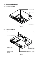


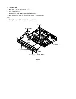

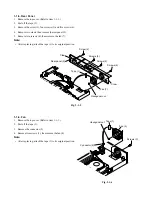

■
DIGITAL AUDIO OUTPUT
BITSTREAM/PCM (OPTICAL terminal)
Optical connector x 1 system
■
DIGITAL AUDIO OUTPUT
BITSTREAM/PCM (COAXIAL terminal)
0.5Vp-p (75
Ω
), pin jack x 1 system
■
CHANNEL CHANGE IR jack
This is for connection of the supplied IR control cable
only.
■
DV input
4-pin x 1 in front
■
Remote control
Wireless remote control (SE-R0132)
■
Operating conditions
Temperature: 5°C ~ 35°C,
Position: Horizontal
■
Clock display
24 hour digital display
■
Clock accuracy
Quartz (monthly deviation: approximately ±30
seconds)
■
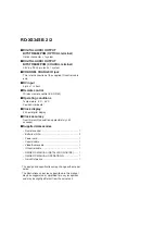
Supplied Accessories
• Remote control ....................................................... 1
• Batteries (R03) ........................................................ 2
• Power cord .............................................................. 1
• Coaxial cable .......................................................... 1
• Video/Audio cable ................................................... 1
• IR control cable ....................................................... 1
• OWNER’S MANUAL (INSTALLATION GUIDE) ....... 1
• OWNER’S MANUAL (OPERATIONS) ..................... 1
• Quick Reference ..................................................... 1
• The design and specifications may change without prior
notice.
• The Illustrations and screens described in this manual
may be exaggerated or simplified for easy recognition
and may be slightly different from the actual unit.
RD-XS34SB 2/2
Содержание RD-XS34SB
Страница 30: ...1 1 SHIBAURA 1 CHOME MINATO KU TOKYO 105 8001 JAPAN ...
Страница 60: ...1 1 SHIBAURA 1 CHOME MINATO KU TOKYO 105 8001 JAPAN ...
Страница 66: ...10 1 3 4 A B C D E G 2 5 6 7 8 9 F Fig 3 4 1 4 CIRCUIT DIAGRAMS 4 1 Power Supply Circuit Diagram ...
Страница 67: ...1 3 4 A B C D E G 2 5 F 4 2 Front Circuit Diagram 4 2 1 Front Jack Circuit Diagram Fig 3 4 2 ...
Страница 68: ...10 1 3 4 A B C D E G 2 5 6 7 8 9 F Fig 3 4 3 4 2 2 Front Circuit Diagram L R ...
Страница 69: ...Fig 3 4 4 4 3 Digital Circuit Diagram 4 3 1 Digital 1 Circuit Diagram ...
Страница 70: ...4 3 Digital Circuit Diagram 4 3 1 Digital 1 Circuit Diagram ...
Страница 71: ......
Страница 72: ......
Страница 73: ......
Страница 74: ......
Страница 75: ......
Страница 76: ......
Страница 77: ...Fig 3 4 4 ...
Страница 78: ...Fig 3 4 5 4 3 2 Digital 2 Circuit Diagram ...
Страница 79: ...4 3 2 Digital 2 Circuit Diagram ...
Страница 80: ......
Страница 81: ......
Страница 82: ......
Страница 83: ......
Страница 84: ...Fig 3 4 5 ...
Страница 85: ...10 1 3 4 A B C D E G 2 5 6 7 8 9 F Fig 3 4 6 4 4 Mother Circuit Diagram 4 4 1 Tuner Interface Circuit Diagram ...
Страница 86: ...10 1 3 4 A B C D E G 2 5 6 7 8 9 F 4 4 2 Timer Circuit Diagram Fig 3 4 7 ...
Страница 87: ...10 1 3 4 A B C D E G 2 5 6 7 8 9 F 4 4 3 Audio Circuit Diagram Fig 3 4 8 TB RDXS34SB TF RDXS34SF TG RDXS34SG ...
Страница 88: ...10 1 3 4 A B C D E G 2 5 6 7 8 9 F 4 4 4 Video Circuit Diagram Fig 3 4 9 DIFFERENCE PARTS FOR RD XS34SF SG ...
Страница 89: ...10 1 3 4 A B C D E G 2 5 6 7 8 9 F Fig 3 4 10 4 4 5 MSP Circuit Diagram ...
Страница 90: ...1 3 4 A B C D E G 2 5 F 4 5 Tuner Unit Circuit Diagram Fig 3 4 11 ...
Страница 95: ...1 2 3 4 5 6 7 A B C D E F 5 6 Mother PC Board Fig 3 5 11 EU05 Mother PC Board Top side ...


