


THCV235_THCV236_Rev.3.40_E
Copyright
©
2016 THine Electronics, Inc.
THine Electronics, Inc.
15/68
Security E
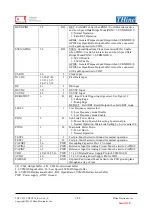
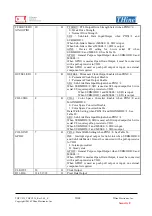
Permanent Clock Output (THCV236 only)
When there is no input from Main-Link, the THCV236 will output internal oscillator clock from CLKOUT pin.
This function is controlled by OUTSEL pin or OUTSEL_ENABLE register and OUTSEL_SETTING register.
See Table 6 and Table 7.
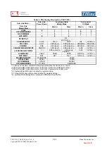
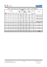
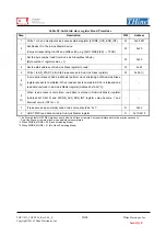
Table 6.
Permanent Clock Output function table (PDN1=0)
OUTSEL (pin)
Output Clock
Frequency
(*1)
0
-
1
40MHz
*1 typical value
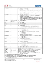
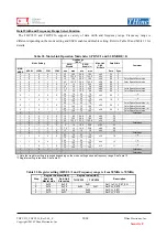
Table 7.
Permanent Clock Output function table (PDN1=1)
OUTSEL_
ENABLE
(register)
OUTSEL_
SETTING
(register)
Output Clock
Frequency
(*1)
0
*
-
1
00
80MHz
01
40MHz(default)
10
20MHz
11
10MHz
*1 typical value
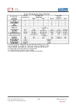
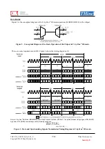
Spread Spectrum Clock Generator (SSCG)
The THCV235 serial data output and the THCV236 parallel data and clock outputs are modulated by
programmable SSCG. The THCV235 SSCG is enabled by SSEN pin or SSEN register. The THCV236 SSCG is
enabled by only SSEN register. The modulation rate and modulation frequency variation of output spread is
controlled through the SSCG control registers on each device. Do not enable spread spectrum for both the
THCV235 and THCV236 at the same time.
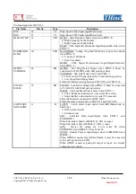
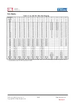
Table 8.
SSCG enable signal (THCV235)
PDN1
SUBMODE
Mode Entry Signal
Description
0
*
(Function as HTPDN)
SSEN (pin)
0:SSCG Disable
1:SSCG Enable
1
0
SSEN
(register)
1
SSEN
(pin)
Table 9.
SSCG enable signal (THCV236)
PDN1
SUBMODE
Mode Entry Signal
Description
* *
SSEN(register)
0:SSCG Disable
1:SSCG Enable


