


Probe Interfaces
10
SPRUI94 – January 2017
Copyright © 2017, Texas Instruments Incorporated
XDS110 Debug Probe
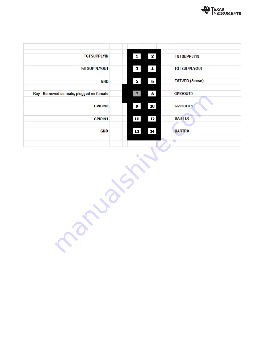
Figure 3. AUX Connection Signal Mapping
A breakout adaptor is also supplied for this interface (see
2.5
Probe Expansion Header
The XDS110 probe also supports an expansion header, for adding functionality to the XDS110 system. It
exposes a number of functional interfaces of the TM4C129 debug control CPU, and these can be utilized
by logic external to the probe. The functional interfaces include:
•
GPIO
•
UART
•
I2C
•
SSI
•
CAN
•
ADC (reference voltage for ADCs is 2.5 V)
•
Timer input
All these interfaces operate at the 3.3 V of the controller, and that voltage is supplied on the connector. A
5-V source is also available for higher voltage needs such as relays.
The expansion port also has interfaces for accepting a power input supplied by the target system, and a
path to send power back to the target system through the XDS110 probe AUX connector. The primary use
case for these features is for energy trace monitoring, but it can be used for other functions.
2.5.1
Physical Connection for the Expansion Interface
The XDS110 probe supports a 30-pin IDC female socket with .100 inch pitch. It exposes additional
functionality of the XDS110 debug processor (TMC4129) for add-on modules. The signal mapping for this
connection is shown in
, but utilizing this interface is generally reserved for TI and designated third
parties that have the ability to integrate the add-on functionality into the entire system.


