GND
1500pF
1500pF
1200pF
1200pF
10pF
680pF
100pF 220pF
680pF
150nH
330nH
GND
GND
27pF
GND
GND
GND
2.2uF
0.01uF
2.2uF
0.01uF
GND
GND
2.2uF
0.01uF
GND
2.2uF
0.01uF
GND
27pF
GND
27pF
GND
1.5uH
68pF
GND
12pF
12pF
6.8k
GND
GND
10k
GND
GND
GND
47k
0.1uF
100R
GND
GND
MC-921
GND
0
0
SMA-142-0701-801/806
GND
057-014-2
2.2uF
0.01uF
GND
C2
C3
C4
C5
C6
C7
C10
C
8
C9
L1
L2
C11
C16
C15
C20
C19
C18
C17
C22
C21
C23
C24
L3
C14
C13
C12
R1
TCK
TMS
P4.0/TB0
P4.1/TB1
P4.2/TB2
P4.3/TB0
P4.4/TB1
P4.5/TB2
P4.6/TBOUTH/ACLK
P4.7/TBCLK
1
2
3
4
5
6
7
8
9
10
11
12
13
14
28
27
26
25
24
23
22
21
20
19
18
17
16
15
29
30
31
32
33
34
35
36
37
38
TP
39
40
R6
R5
C1
R4
X2
R2
R3
GND1
2
IN
1
GND2
4
OUT
3
X3
V
D
D
_
X
3
2
O
S
C
_
IN
3
1
O
S
C
_
O
U
T
3
0
V
S
S
_
D
2
9
E
N
2
8
S
Y
S
_
C
L
K
2
7
D
A
T
A
_
C
L
K
2
6
E
N
2
2
5
I/O_7
24
I/O_6
23
I/O_5
22
I/O_4
21
I/O_3
20
I/O_2
19
VDD_A
1
VIN
2
VDD_PA
4
TX_OUT
5
VSS_PA
6
VDD_RF
3
I/O_1
18
I/0_0
17
B
A
N
D
_
G
A
P
11
V
D
D
_
I/
O
1
6
V
S
S
_
A
1
5
M
O
D
1
4
IRQ
1
3
A
S
K
/O
O
K
1
2
VSS_RX
7
RX_IN1
8
V
S
S
1
0
RX
_IN2
9
GND(PAD)
33
X4-1
X4
-2
X4-3
X4
-4
X4-5
X4
-6
X4-7
X4
-8
X4-9
X4
-10
X4-11
X
4-12
X4-13
X
4-14
C25
C26
SYS_CLK
S
Y
S
_
C
L
K
DATA_CLK
D
A
T
A
_
C
L
K
VIN
V
IN
IRQ
IRQ
M
O
D
MOD
V
D
D
_
X
V
D
D
_
X
RST_NMI
RST_NMI
RST_NMI
TCK
TCK
TMS
TMS
TDI
TDI
TDO/TDI
TDO/TDI
VCC
VCC
VCC
VCC
RXD
TXD
ASK/OOK
A
S
K
/O
O
K
E
N
EN
OSC_OUT
O
S
C
_
O
U
T
O
S
C
_
IN
OSC_IN
JTAG
(+2.7VDC - 5.5VDC)
TRF7964A
SLOS787H – MAY 2012 – REVISED APRIL 2014
7
Application Schematic and Layout Considerations
7.1
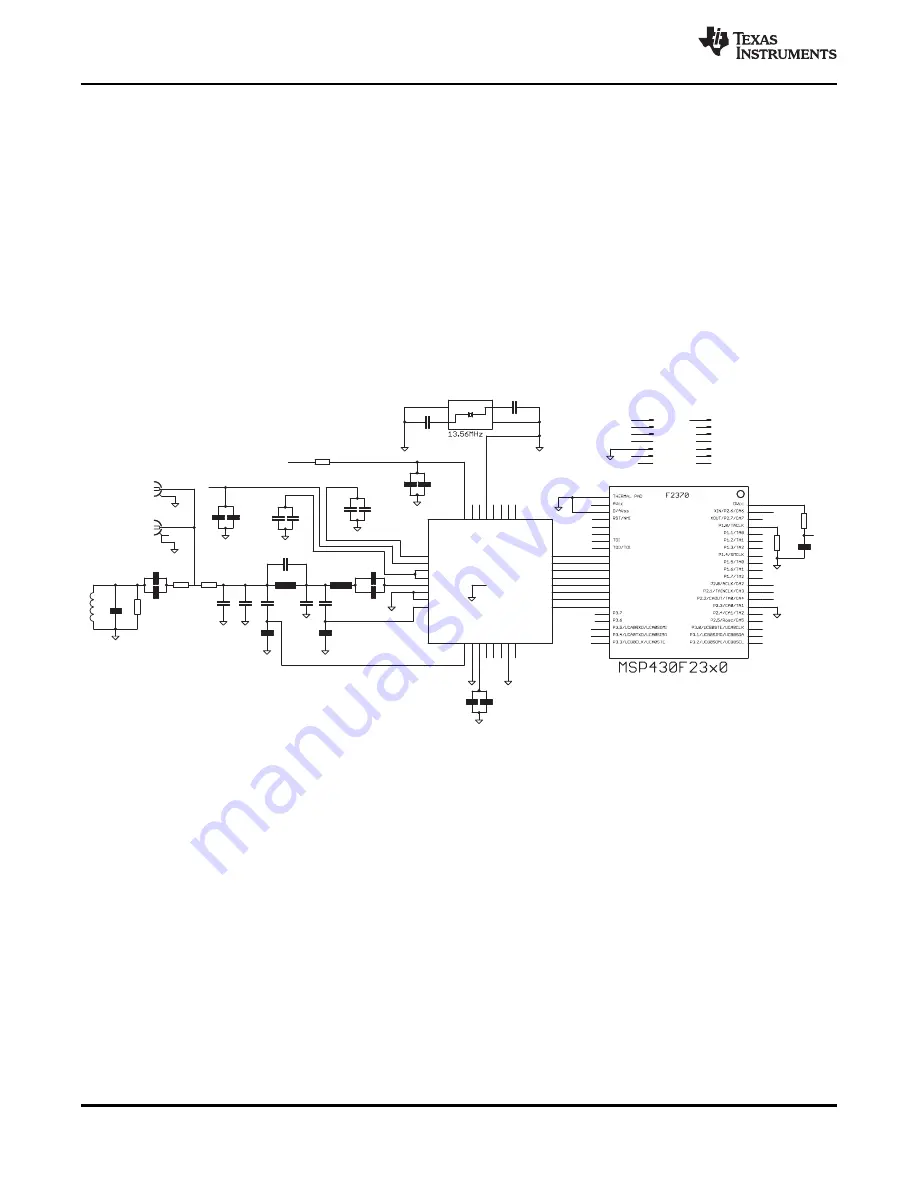
TRF7964A Reader System Using Parallel Microcontroller Interface
7.1.1
General Application Considerations
shows the most flexible TRF7964A application schematic. Both ISO15693, ISO14443 and
FeliCa systems can be addressed. Due to the low clock frequency on the DATA_CLK line, the parallel
interface is the most robust way to connect the TRF7964A with the MCU.
shows matching to a 50-
Ω
port, which allows connecting to a properly matched 50-
Ω
antenna
circuit or RF measurement equipment (for example, a spectrum analyzer or power meter).
7.1.2
Schematic
shows a sample application schematic for a parallel MCU interface.
Figure 7-1. Application Schematic – Parallel MCU Interface
An MSP430F2370 (32KB Flash, 2KB RAM) is shown in
. Minimum MCU requirements depend
on application requirements and coding style. If only one ISO protocol or a limited command set of a
protocol needs to be supported, MCU Flash and RAM requirements can be significantly reduced. Be
aware that recursive inventory and anticollision commands require more RAM than single slotted
operations. For example, current reference firmware for ISO15693 (with host interface) is approximately
8KB, using 512B RAM; for all supported protocols (also with same host interface) the reference firmware
is approximately 12KB and uses a minimum of 1KB RAM. An MCU capable of running its GPIOs at
13.56 MHz is required for Direct Mode 0 operations.
68
Application Schematic and Layout Considerations
Copyright © 2012–2014, Texas Instruments Incorporated
Product Folder Links:


