3.2.1.2
Power/Suspend Switches
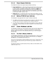
The notebook contains two power/mode switches including:
•
Power On/Off
Switch- Horizontal slide type switch that controls power
to the unit (left most position is Off). When initially set to the On (
I
)
position, power is applied to the Notebook Computer, the
PWR
LED
glows green and the computer executes power up self test; then loads
Windows. When set to the
O
or Off position, the Notebook powers down
and all data in RAM memory is lost.
•
Suspend
Switch- an alternate action touch switch that places the unit
in Suspend Mode (if previously On) or On if previously in Suspend Mode.
3.2.1.3
Battery/PCMCIA Eject Switches
The Notebook is equipped with four "eject" switches including:
•
Two Battery Eject switches (just above the keyboard on left side). These
switches slide to the left to release the two notebook batteries.
•
Two PCMCIA Card Eject switches (above the keyboard on the right side
of the unit). These switches are used to release the two PCMCIA cards,
if installed.
3.2.2
Cover Release Latches
The Notebook contains two Cover Release latches (right and left edges of top
cover). To open the notebook, simultaneously slide both release latches
forward (toward the front of the notebook) and lift up on the front edge of
the top cover.
3.2.2.1
The Point (Mouse) Switches
The TM5000 Series Notebook Computers are equipped with a built-in mouse
device called "the Point" physically located at the intersection of the
G, H,
and
B
keys on the keyboard (see Figure 3-2).
The cursor is positioned by applying slight pressure to the rubber ball in the
direction you want the cursor to go. The harder you press, the faster the
cursor moves.
The select functions are performed by the two buttons at the bottom of the
keyboard (Figure 3-2).
Operating Instructions
3-3
Содержание TravelMate 5000 Series
Страница 1: ...Maintenance Manual TravelMate 5000 Series Notebook Computers 9786166 0001 March 1995 ...
Страница 47: ...Figure 1 16 TM5000 Series Functional Block Diagram 1 30 General Description ...
Страница 95: ...Figure 4 2 Notebook Detailed Block Diagram Troubleshooting Procedures 4 3 ...
Страница 149: ...Figure 6 4 Main Board P54 75MHz P N 9798803 0001 Sheet 2 of 2 6 14 Illustrated Parts Listing ...
Страница 161: ...Figure 6 5 Figure 6 5 PCMCIA Sound Board P N 9786205 0001 Sheet 1 of 2 6 26 Illustrated Parts Listing ...
Страница 162: ...Figure 6 6 Figure 6 5 PCMCIA Sound Board P N 9786205 0001 Sheet 2 of 2 Illustrated Parts Listing 6 27 ...
Страница 172: ...Figure 6 7 Keyscan Board P N 9786209 0001 Illustrated Parts Listing 6 37 ...
Страница 180: ...Figure 6 11 Inverter Board P N 9786134 0001 Illustrated Parts Listing 6 45 ...
Страница 185: ...Figure 6 12 DAB Board P N 9786273 0001 6 50 Illustrated Parts Listing ...
Страница 188: ...Figure 7 1 Figure 7 1 Main Board Part No 9798803 Logic Diagram Sheet 1 of 22 7 2 Schematic Diagrams ...
Страница 189: ...Figure 7 1 Figure 7 1 Main Board Part No 9798803 Logic Diagram Sheet 2 of 22 Schematic Diagrams 7 3 ...
Страница 190: ...Figure 7 1 Figure 7 1 Main Board Part No 9798803 Logic Diagram Sheet 3 of 22 7 4 Schematic Diagrams ...
Страница 191: ...Figure 7 1 Figure 7 1 Main Board Part No 9798803 Logic Diagram Sheet 4 of 22 Schematic Diagrams 7 5 ...
Страница 192: ...Figure 7 1 Figure 7 1 Main Board Part No 9798803 Logic Diagram Sheet 5 of 22 7 6 Schematic Diagrams ...
Страница 193: ...Figure 7 1 Figure 7 1 Main Board Part No 9798803 Logic Diagram Sheet 6 of 22 Schematic Diagrams 7 7 ...
Страница 194: ...Figure 7 1 Figure 7 1 Main Board Part No 9798803 Logic Diagram Sheet 7 of 22 7 8 Schematic Diagrams ...
Страница 195: ...Figure 7 1 Figure 7 1 Main Board Part No 9798803 Logic Diagram Sheet 8 of 22 Schematic Diagrams 7 9 ...
Страница 196: ...Figure 7 1 Figure 7 1 Main Board Part No 9798803 Logic Diagram Sheet 9 of 22 7 10 Schematic Diagrams ...
Страница 197: ...Figure 7 1 Figure 7 1 Main Board Part No 9798803 Logic Diagram Sheet 10 of 22 Schematic Diagrams 7 11 ...
Страница 198: ...Figure 7 1 Figure 7 1 Main Board Part No 9798803 Logic Diagram Sheet 11 of 22 7 12 Schematic Diagrams ...
Страница 199: ...Figure 7 1 Figure 7 1 Main Board Part No 9798803 Logic Diagram Sheet 12 of 22 Schematic Diagrams 7 13 ...
Страница 200: ...Figure 7 1 Figure 7 1 Main Board Part No 9798803 Logic Diagram Sheet 13 of 22 7 14 Schematic Diagrams ...
Страница 201: ...Figure 7 1 Figure 7 1 Main Board Part No 9798803 Logic Diagram Sheet 14 of 22 Schematic Diagrams 7 15 ...
Страница 202: ...Figure 7 1 Figure 7 1 Main Board Part No 9798803 Logic Diagram Sheet 15 of 22 7 16 Schematic Diagrams ...
Страница 203: ...Figure 7 1 Figure 7 1 Main Board Part No 9798803 Logic Diagram Sheet 16 of 22 Schematic Diagrams 7 17 ...
Страница 204: ...Figure 7 1 Figure 7 1 Main Board Part No 9798803 Logic Diagram Sheet 17 of 22 7 18 Schematic Diagrams ...
Страница 205: ...Figure 7 1 Figure 7 1 Main Board Part No 9798803 Logic Diagram Sheet 18 of 22 Schematic Diagrams 7 19 ...
Страница 206: ...Figure 7 1 Figure 7 1 Main Board Part No 9798803 Logic Diagram Sheet 19 of 22 7 20 Schematic Diagrams ...
Страница 207: ...Figure 7 1 Figure 7 1 Main Board Part No 9798803 Logic Diagram Sheet 20 of 22 Schematic Diagrams 7 21 ...
Страница 208: ...Figure 7 1 Figure 7 1 Main Board Part No 9798803 Logic Diagram Sheet 21 of 22 7 22 Schematic Diagrams ...
Страница 209: ...To Be Supplied Figure 7 1 Figure 7 1 Main Board Part No 9798803 Logic Diagram Sheet 22 of 22 Schematic Diagrams 7 23 ...
Страница 210: ...Figure 7 2 Figure 7 2 PCMCIA Sound Board P N 9786205 Logic Diagram Sheet 1 of 12 7 24 Schematic Diagrams ...
Страница 211: ...Figure 7 2 Figure 7 2 PCMCIA Sound Board P N 9786205 Logic Diagram Sheet 2 of 12 Schematic Diagrams 7 25 ...
Страница 212: ...Figure 7 2 Figure 7 2 PCMCIA Sound Board P N 9786205 Logic Diagram Sheet 3 of 12 7 26 Schematic Diagrams ...
Страница 213: ...Figure 7 2 Figure 7 2 PCMCIA Sound Board P N 9786205 Logic Diagram Sheet 4 of 12 Schematic Diagrams 7 27 ...
Страница 214: ...Figure 7 2 Figure 7 2 PCMCIA Sound Board P N 9786205 Logic Diagram Sheet 5 of 12 7 28 Schematic Diagrams ...
Страница 215: ...Figure 7 2 Figure 7 2 PCMCIA Sound Board P N 9786205 Logic Diagram Sheet 6 of 12 Schematic Diagrams 7 29 ...
Страница 216: ...Figure 7 2 Figure 7 2 PCMCIA Sound Board P N 9786205 Logic Diagram Sheet 7 of 12 7 30 Schematic Diagrams ...
Страница 217: ...Figure 7 2 Figure 7 2 PCMCIA Sound Board P N 9786205 Logic Diagram Sheet 8 of 12 Schematic Diagrams 7 31 ...
Страница 218: ...Figure 7 2 Figure 7 2 PCMCIA Sound Board P N 9786205 Logic Diagram Sheet 9 of 12 7 32 Schematic Diagrams ...
Страница 219: ...Figure 7 2 Figure 7 2 PCMCIA Sound Board P N 9786205 Logic Diagram Sheet 10 of 12 Schematic Diagrams 7 33 ...
Страница 220: ...Figure 7 2 Figure 7 2 PCMCIA Sound Board P N 9786205 Logic Diagram Sheet 11 of 12 7 34 Schematic Diagrams ...
Страница 221: ...Figure 7 2 Figure 7 2 PCMCIA Sound Board P N 9786205 Logic Diagram Sheet 12 of 12 Schematic Diagrams 7 35 ...
Страница 222: ...Figure 7 3 Figure 7 3 Keyscan Board P N 9786209 Logic Diagram Sheet 1 of 5 7 36 Schematic Diagrams ...
Страница 223: ...Figure 7 3 Figure 7 3 Keyscan Board P N 9786209 Logic Diagram Sheet 2 of 5 Schematic Diagrams 7 37 ...
Страница 224: ...Figure 7 3 Figure 7 3 Keyscan Board P N 9786209 Logic Diagram Sheet 3 of 5 7 38 Schematic Diagrams ...
Страница 225: ...Figure 7 3 Figure 7 3 Keyscan Board P N 9786209 Logic Diagram Sheet 4 of 5 Schematic Diagrams 7 39 ...
Страница 226: ...Figure 7 3 Figure 7 3 Keyscan Board P N 9786209 Logic Diagram Sheet 5 of 5 7 40 Schematic Diagrams ...
Страница 227: ...Figure 7 4 Figure 7 4 Sleep Switch Board P N 9786148 Logic Diagram Sheet 1 of 1 Schematic Diagrams 7 41 ...
Страница 228: ...Figure 7 5 Figure 7 5 IR Board P N 9798813 Logic Diagram Sheet 1 of 2 7 42 Schematic Diagrams ...
Страница 229: ...Figure 7 5 Figure 7 5 IR Board P N 9798813 Logic Diagram Sheet 2 of 2 Schematic Diagrams 7 43 ...
Страница 230: ...Figure 7 6 Figure 7 6 LED Board P N 9796128 Logic Diagram Sheet 1 of 2 7 44 Schematic Diagrams ...
Страница 231: ...Figure 7 6 Figure 7 6 LED Board P N 9796128 Logic Diagram Sheet 2 of 2 Schematic Diagrams 7 45 ...
Страница 232: ...Figure 7 7 Figure 7 7 8 16 MB RAM Exp Board P N 9798816 Logic Diagram Sheet 1 of 1 7 46 Schematic Diagrams ...
Страница 233: ...Figure 7 8 Figure 7 8 Inverter Board P N 9796134 Logic Diagram Sheet 1 of 2 Schematic Diagrams 7 47 ...
Страница 234: ...Figure 7 8 Figure 7 8 Inverter Board P N 9796134 Logic Diagram Sheet 2 of 2 7 48 Schematic Diagrams ...
Страница 235: ...Figure 7 8 Figure 7 9 Display Adapter Board P N 9786273 Logic Diagram Sheet 1 of 3 Schematic Diagrams 7 49 ...
Страница 236: ...Figure 7 9 Figure 7 9 Display Adapter Board P N 9786273 Logic Diagram Sheet 2 of 3 7 50 Schematic Diagrams ...
Страница 237: ...Figure 7 9 Figure 7 9 Display Adapter Board P N 9786273 Logic Diagram Sheet 3 of 3 Schematic Diagrams 7 51 ...
Страница 239: ...Figure A 1 Code Page 437 United States A 2 Character Sets ...
Страница 240: ...Figure A 2 Code Page 850 Multilingual Character Sets A 3 ...
Страница 241: ...Figure A 3 Code Page 863 Canadian French A 4 Character Sets ...
Страница 242: ...Figure A 4 Code Page 865 Nordic Character Sets A 5 ...
Страница 286: ...Printed in U S A ...


