Board Layout
www.ti.com
6
SLVUAU1 – October 2016
Submit Documentation Feedback
Copyright © 2016, Texas Instruments Incorporated
TPD8S300 Evaluation Module
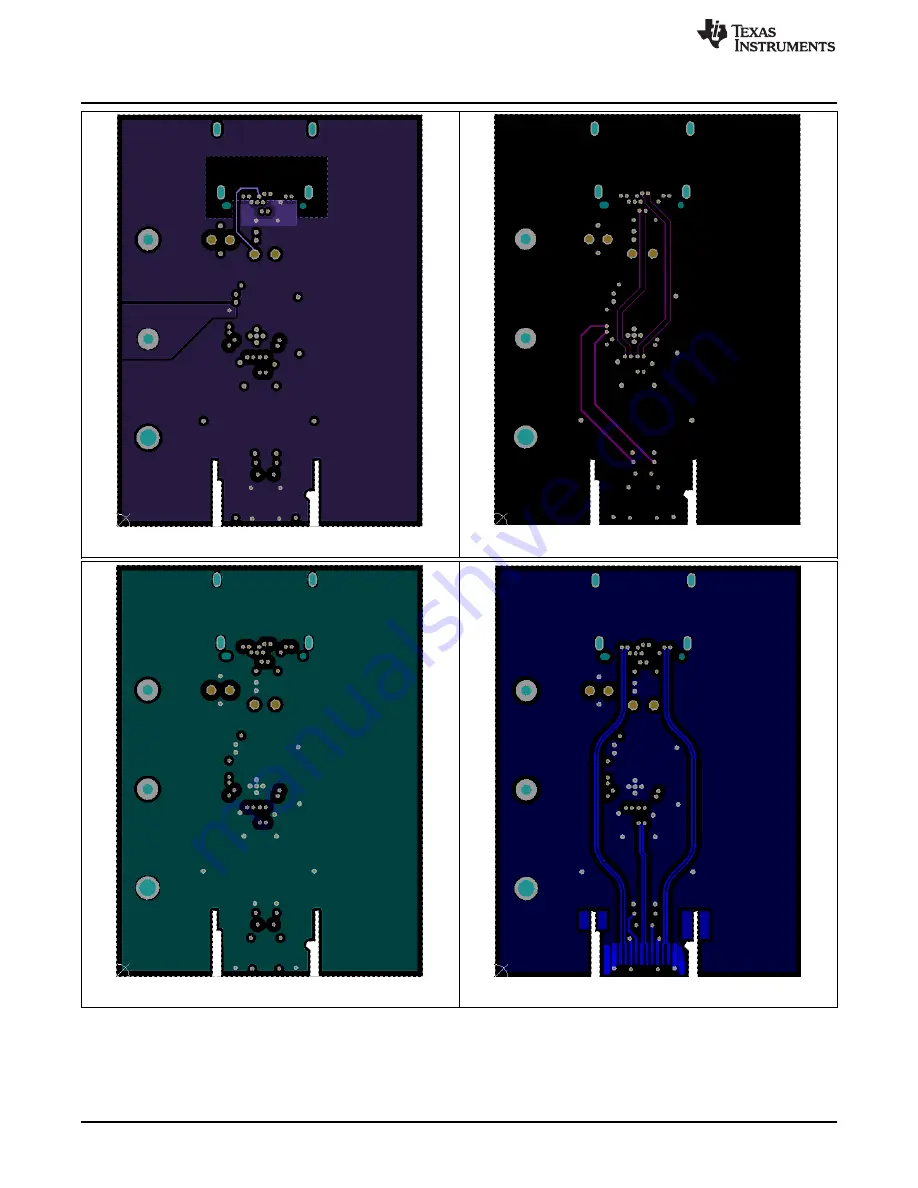
Figure 8. Power Plane 1
Figure 9. Midlayer 2
Figure 10. Ground Plane 3
Figure 11. Bottom Layer
Страница 1: ...00 overvoltage protection and ESD protection in their own system This user s guide includes setup instructions schematic diagrams a bill of materials and printed circuit board layout drawings for the...
Страница 2: ...ctionality by manually removing these resistors The EVM requires 3 3 V between the Vpwr TP1 and Ground TP3 pins to power up the TPD8S300 If the system supports USB charging from a dead battery conditi...
Страница 3: ...D simulator in either contact or air gap test mode to measure the ESD protection provided by the TPD8S300 Probe points one and two correspond to the SBU2 and SBU1 lines respectively Probe points four...
Страница 4: ...Schematic www ti com 4 SLVUAU1 October 2016 Submit Documentation Feedback Copyright 2016 Texas Instruments Incorporated TPD8S300 Evaluation Module 3 Schematic Figure 3 TPD8S300EVM Schematic...
Страница 5: ...right 2016 Texas Instruments Incorporated TPD8S300 Evaluation Module 4 Board Layout This section provides the TPD8S300EVM board layout The TPD8S300 is an 8 layer board of FR 4 at 0 032 thickness Figur...
Страница 6: ...com 6 SLVUAU1 October 2016 Submit Documentation Feedback Copyright 2016 Texas Instruments Incorporated TPD8S300 Evaluation Module Figure 8 Power Plane 1 Figure 9 Midlayer 2 Figure 10 Ground Plane 3 Fi...
Страница 7: ...Plug USB3 1 Type C 24 V Position R A SMT DX07P024MJ1R15 00 JAE Electronics J2 1 Receptacle 0 5 mm USB TYPE C R A SMT Receptacle 5mm USB TYPE C R A SMT 12401610E4 2A Amphenol Canada R1 1 100 k RES 100...
Страница 8: ...sponsible for compliance with all legal regulatory and safety related requirements concerning its products and any use of TI components in its applications notwithstanding any applications related inf...