GPMC_FCLK
D[15:0]
WAIT
Data 0
Data 1
First read access
Second read access
OEOFFTIME
RDCYCLETIME
OEONTIME = 0
CSRDOFFTIME
CSONTIME = 0
OEONTIME = 0
CSONTIME = 0
RDACCESSTIME
nBE0/CLE
nCS
nOE/nRE
nADV/ALE
OEOFFTIME − x clk cycles
RDACCESSTIME - x clk cycles
RDCYCLETIME − x clk cycles
CSRDOFFTIME − x clk cycles
x is the programmed value in the
GPMC_PREFETCH_CONFIG1[30:28]
CYCLEOPTIMIZATION field
Preliminary
Architecture
www.ti.com
5.2.4.12.4.6 Optimizing NAND Access Using the Prefetch and Write-Posting Engine
Access time to a NAND memory device can be optimized for back-to-back accesses if the associated
CS signal is not deasserted between accesses. The GPMC access engine can track prefetch engine
accesses to optimize the access timing parameter programmed for the allocated chip-select, if no
accesses to other chip-selects (that is, interleaved accesses) occur. Similarly, the access engine also
eliminates the CYCLE2CYCLEDELAY even if CYCLE2CYCLESAMECSEN is set. This capability is
limited to the prefetch and write-posting engine accesses, and MPU accesses to a NAND memory
device (through the defined chip-select memory region or through the GPMC_NAND_DATA_i(where , i
= 0 to 7) are never optimized.
The GPMC_PREFETCH_CONFIG1[27] ENABLEOPTIMIZEDACCESS bit must be set to enable
optimized accesses. To optimize access time, the GPMC_PREFETCH_CONFIG1[30-28]
CYCLEOPTIMIZATION field defines the number of GPMC_FCLK cycles to be suppressed from the
RDCYCLETIME, WRCYCLETIME, RDACCESSTIME, WRACCESSTIME, CSOFFTIME, ADVOFFTIME,
OEOFFTIME, and WEOFFTIME timing parameters.
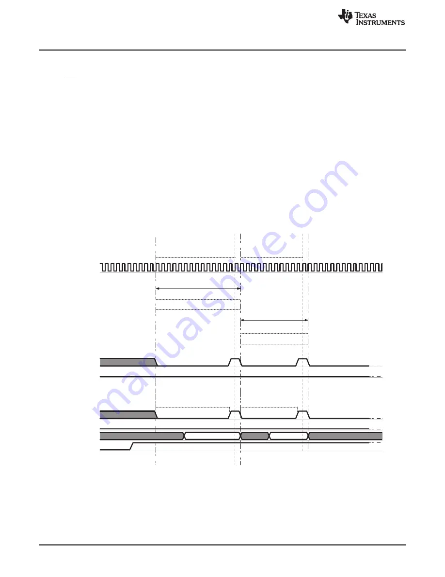
, in the case of back-to-back accesses to the NAND flash through the prefetch engine,
CYCLE2CYCLESAMECSEN is forced to 0 when using optimized accesses. The first access uses the
regular timing settings for this chip-select. All accesses after this one use settings reduced by x clock
cycles, x being defined by the GPMC_PREFETCH_CONFIG1[30-28] CYCLEOPTIMIZATION field.
Figure 5-41. NAND Read Cycle Optimization Timing Description
632
General-Purpose Memory Controller (GPMC)
SPRUGX9 – 15 April 2011
© 2011, Texas Instruments Incorporated
Содержание TMS320C6A816 Series
Страница 2: ...Preliminary 2 SPRUGX9 15 April 2011 Submit Documentation Feedback 2011 Texas Instruments Incorporated...
Страница 92: ...92 Read This First SPRUGX9 15 April 2011 Submit Documentation Feedback 2011 Texas Instruments Incorporated...
Страница 1122: ...1122 Multichannel Audio Serial Port McASP SPRUGX9 15 April 2011 Submit Documentation Feedback 2011 Texas Instruments Incorporated...
Страница 1562: ...1562 Real Time Clock RTC SPRUGX9 15 April 2011 Submit Documentation Feedback 2011 Texas Instruments Incorporated...
Страница 1658: ...1658 Timers SPRUGX9 15 April 2011 Submit Documentation Feedback 2011 Texas Instruments Incorporated...
Страница 1750: ...1750 UART IrDA CIR Module SPRUGX9 15 April 2011 Submit Documentation Feedback 2011 Texas Instruments Incorporated...
Страница 1984: ...1984 Universal Serial Bus USB SPRUGX9 15 April 2011 Submit Documentation Feedback 2011 Texas Instruments Incorporated...


