background image

Input and Output Setup for Channel 2

2-6

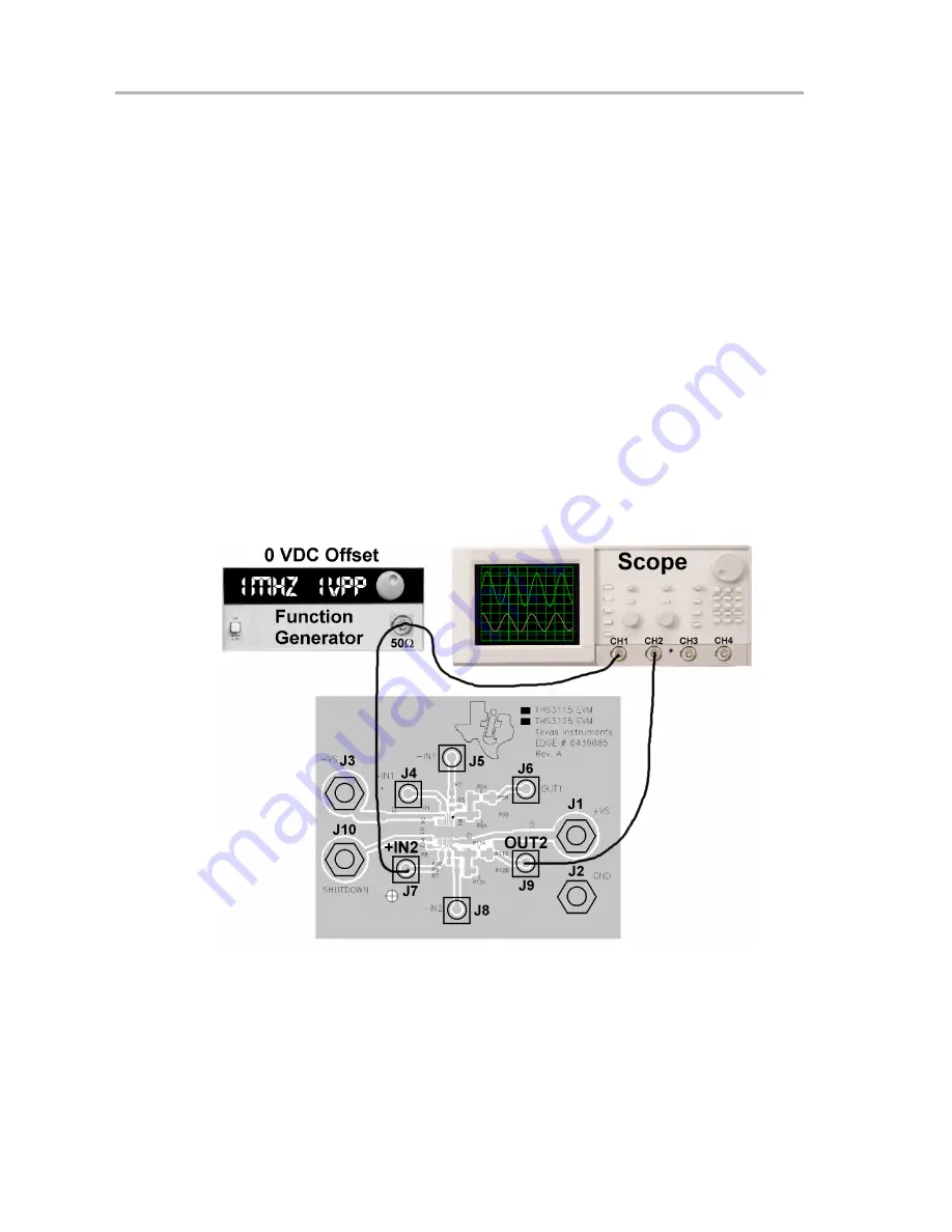
2.5 Input and Output Setup for Channel 2

1) Verify that the function generator is still set to generate a 1-MHz,

±

0.5 V

(1-V

PP

) sine wave with no dc offset.

2) Turn off the function generator before proceeding to the next step.
3) Connect a BNC

T

connector to the output of the function generator.

4) Using a BNC-to-SMA cable, connect the function generator to J7 (+IN2)

on the EVM.

5) Using a BNC-to-BNC cable, connect the function generator output to the

oscilloscope input 1.

NOTE

:

The oscilloscope input 1 must be set to use 1-M

W

input impedance for

proper results.
6) Using a BNC-to-SMA cable, connect the oscilloscope input 2 to J9 (OUT2)

on the EVM.

7) Set the oscilloscope to 0.2 V/division and a time-base of 0.1

m

s/division.

NOTE:

The oscilloscope input 2 must be set to use 50-

W

input impedance for

proper results.

Figure 2--5. Signal Connections for Channel 2

Содержание THS3115 EVM

Страница 1: ...THS3115 25 EVM May 2002 HPL User s Guide SLOU126 ...

Страница 2: ...present that any license either express or implied is granted under any TI patent right copyright maskworkright orotherTIintellectualproperty rightrelating toany combination machine orprocess in which TIproducts orservices are used Information published by TIregarding third party products orservices does not constitute a license from TI to use such products or services or a warranty or endorsement...

Страница 3: ...ing from the handling or use of the goods Please be aware that the products received may not be regulatory compliant or agency certified FCC UL CE etc Due to the open construction oftheproduct itistheuser sresponsibilitytotakeanyandall appropriateprecautions withregard toelectrostatic discharge EXCEPT TO THE EXTENT OF THE INDEMNITY SET FORTH ABOVE NEITHER PARTY SHALL BE LIABLE TO THE OTHER FOR ANY...

Страница 4: ...re is uncertainty as to the load specification please contact a TI field representative During normal operation some circuitcomponents may have case temperatures greaterthan 60 C The EVM is designed to operate properly with certain components above 60 C as long as the input and output ranges are maintained These components include but are not limited tolinearregulators switchingtransistors passtra...

Страница 5: ...o determine the design techniques used in the evaluation board It is recommended that the user review the application notes Current Feedback Amplifier Analysis and Compensation literature number SLOA021A and Voltage Feedback vs Current Feedback Op Amps literature number SLVA051 to gain more insight about current feedback amplifiers How to Use This Manual This document contains the following chapte...

Страница 6: ... sc psheets slva051 slva051 pdf Application report literature number SLOA069 How Not to Decouple High Speed Op Amp Circuits http www s ti com sc psheets sloa069 sloa069 pdf Application report literature number SLOA072 Single Supply Differential Op Amp Techniques http www s ti com sc psheets sloa072 sloa072 pdf FCC Warning This equipment is intended for use in a laboratory test environment only It ...

Страница 7: ...Input and Output Setup for Channel 1 2 3 2 4 Operating the EVM on Channel 1 2 4 2 5 Input and Output Setup for Channel 2 2 6 2 6 Operating the EVM on Channel 2 2 7 3 Circuit Design Examples 3 1 3 1 Inverting Stage Channel 1 Operation 3 2 3 2 Noninverting Stage Channel 2 Operation 3 4 3 3 Shut Down Operation Channels 1 and 2 3 4 4 General High Speed Amplifier Design Considerations 4 1 5 EVM Hardwar...

Страница 8: ... 1 With Shutdown Activated 2 5 2 5 Signal Connections for Channel 2 2 6 2 6 Oscilloscope Output for Channel 2 2 7 2 7 Oscilloscope Output for Channel 2 With Shutdown Activated 2 8 3 1 Inverting Gain Stage 3 2 3 2 Noninverting Gain Stage 3 4 5 1 Top Layer 1 Signals for THS3115 EVM 5 4 5 2 Bottom Layer 2 Ground and SIgnal for THS3115 EVM 5 5 5 3 Full Schematic of the EVM 5 6 Tables 5 1 THS3115 EVM B...

Страница 9: ... high speed amplifier design considerations This EVM enables the user to implement various circuits to clarify the available configurations presented in the schematic of the EVM In addition when the customer receives the EVM the schematic of the default circuit has been added to depict the components mounted on the EVM Other sample circuits are presented for user implementation The user is not lim...

Страница 10: ... R5A and R11A 100 W 1 watt output load resistors R6B and R12B Footprints are provided for lower power resistors R6A and R12A Shut down SD pin control J10 Power supply ripple rejection capacitors C1 and C2 Decoupling capacitors C3 C4 populated with 0 1 mF capacitors Design final decoupling in accordance with SLOA069 A good example of high speed amplifier PCB design and layout 1 3 THS3115 25 EVM Ope...

Страница 11: ...er 4 for clarity In addition only the components associated with the section of the IC being used A or B are shown Figure 1 1 Schematic of the Populated Circuit on the EVM Default Configuration R11B 49 9W J6 OUT1 J1 VS C3 0 1mF J8 IN2 J4 C4 0 1mF VS C2 6 8mF J2 GND R5B 49 9W R10 909W VS SD U1A THS31x5PWP 2 3 14 4 1 9 6 R3 750W J5 IN1 R6B 100W R1 0 R13 0 VS R9 909W R8 49 9W J3 VS R4 750W J7 IN2 R12...

Страница 12: ...about the various terminals on the EVM and their function In addition it lists the components and equipment needed to operate the EVM Topic Page 2 1 Required Equipment 2 2 2 2 Power Supply Setup for 15 Vdc 2 2 2 3 Input and Output Setup for Channel 1 2 3 2 4 Operating the EVM on Channel 1 2 4 2 5 Input and Output Setup for Channel 2 2 6 2 6 Operating the EVM on Channel 2 2 7 Chapter 2 ...

Страница 13: ...Set the dc power supply to 15 V 2 Make sure the dc power supply is turned off before proceeding to the next step 3 Connect the positive terminal of the power supply to the positive terminal of the current meter number 1 4 Connect the negative terminal of the current meter number 1 to the VS terminal of the EVM J1 5 Connect the common ground terminal of the power supply to the ground GND terminal o...

Страница 14: ...to the output of the function generator 4 Using a BNC to SMA cable connect the function generator to J5 IN1 on the EVM 5 Using a BNC to BNC cable connect the function generator output to the oscilloscope input 1 NOTE The oscilloscope input 1 must be set to use 1 MW input impedance for proper results 6 Using a BNC to SMA cable connect the oscilloscope to J6 OUT1 on the EVM 7 Set the oscilloscope to...

Страница 15: ...A Currents above the limits stated above indicate a possible short or a wrong resistor value on the PCB Do not proceed until this situation is correct 3 Turn on the function generator 4 Verify the oscilloscope is showing two 1 MHz sine waves the input with an amplitude of 0 484 V and the output with an amplitude of 0 242 V as shown in Figure 2 3 They should be 180 out out of phase See Section 3 1 ...

Страница 16: ...4 Turn off the supply 7 Disconnect the shutdown supply from the EVM 8 Set the shutdown supply to 5 V but turn it off during the next step 9 Reconnect the shutdown supply to the EVM 10 Turn on the shutdown supply and verify that the output goes to a straight line as shown in Figure 2 4 centered on zero volts and the current on both current meters indicate below 5 mA Figure 2 4 Oscilloscope Output f...

Страница 17: ...BNC to SMA cable connect the function generator to J7 IN2 on the EVM 5 Using a BNC to BNC cable connect the function generator output to the oscilloscope input 1 NOTE The oscilloscope input 1 must be set to use 1 MW input impedance for proper results 6 Using a BNC to SMA cable connect the oscilloscope input 2 to J9 OUT2 on the EVM 7 Set the oscilloscope to 0 2 V division and a time base of 0 1 ms ...

Страница 18: ...hould have amplitude of 0 5 V and both should be in phase Figure 2 6 Oscilloscope Output for Channel 2 600 m 400 m 200 m 0 200 m 400 m 600 m 0 500 n 1 ms Voltage V t Time s INPUT and OUTPUT 5 Set the shutdown supply to 0 V but leave it off 6 Turn on the single 5 V power supply and verify that the output is unchanged from step 4 Turn off the supply 7 Disconnect the shutdown supply from the EVM 8 Se...

Страница 19: ...Operating the EVM on Channel 2 2 8 Figure 2 7 Oscilloscope Output for Channel 2 With Shutdown Activated 600 m 400 m 200 m 0 200 m 400 m 600 m 0 500 n 1 ms Voltage V t Time s INPUT OUTPUT ...

Страница 20: ...o the user but many other circuits can be constructed The user is encouraged to experiment with different circuits exploring new and creative design techniques That after all is the function of an evaluation board Topic Page 3 1 Inverting Stage Channel 1 Operation 3 2 3 2 Noninverting Stage Channel 2 Operation 3 4 3 3 Shut Down Operation Channels 1 and 2 3 4 Chapter 3 ...

Страница 21: ...affects the level of voltage applied to the EVM While the function generator indicates a level of 0 5 V 1 VPP only 0 484 V 0 968 VPP is applied to the board The user is justified in wondering what happened where did the rest of the voltage 0 016 V go There are two ways of looking at this problem From the function generator side The function generator contains a 50 W source resistor The EVM contain...

Страница 22: ...he source at J4 of the EVM From the EVM side The Thevenin equivalent resistance of the EVM plus the source looking towards the source from the inverting input of the op amp is Rth Rg Rsource Rtermination Rsource Rtermination 750 50 49 9 50 49 9 774 97 W Therefore the inverting gain on a 0 5 Vpeak ideal voltage source assumed to be embedded in the function generator is Voutput Vin Rf Rg 0 5 750 774...

Страница 23: ...ting Gain Stage J9 OUT2 R12B 100W J7 IN2 R8 49 9W R10 909W R9 909W R7 0 R11B 49 9W U1B THS31x5PWP 12 11 13 The gain of the circuit as populated is 2 with a high impedance load and 1 with a 50 W load This circuit does not exhibit the reduction in input voltage level described for the inverting stage as the input is connected directly to a high impedance input of the op amp The circuit of Figure 3 2...

Страница 24: ...aced as close as possible to the IC power input pins in order to minimize the return path impedance This improves high frequency bypassing and reduces harmonic distortion If poor high frequency performance is observed replace the 0 1 mF capacitors with microwave capacitors with a self resonance at the frequency that produces trouble A proper ground plane on both sides of the PCB should be used wit...

Страница 25: ...mination of all inputs and outputs must be incorporated into the layout Unterminated lines such as coaxial cable can appear to be a reactive load to the amplifier By terminating a transmission line with its characteristic impedance the amplifier s load then appears to be purely resistive and reflections are absorbed at each end of the line Another advantage of using an output termination resistor ...

Страница 26: ...ardware Description This chapter describes the EVM hardware It includes the EVM parts list the printed circuit board layout and the schematic Topic Page 5 1 Bill of Materials 5 2 5 2 Circuit Board Layout 5 4 5 3 Schematic 5 6 Chapter 5 ...

Страница 27: ...arrett 9C08052A9090FKHFT 6 OPEN 1206 R5A R6A R11A R12A 4 7 Resistor 0 W 1 4W 1206 R1 R7 2 Phycomp 9C12063A0R00JLHFT Garrett 9C12063A0R00JLHFT 8 Resistor 49 9 W 1 4W 1 1206 R2 R8 2 Phycomp 9C12063A49R9FKRFT Garrett 9C12063A49R9FKRFT 9 Resistor 49 9 W 1W 1 2512 R5B R11B 2 Vishay CRCW251249R9FP KOA RK73H3A49R9FP TTI CRCW251249R9FP TTI RK73H3A49R9FP 10 Resistor 100 W 1W 1 2512 R6B R12B 2 KOA RK73H3A10...

Страница 28: ... Garrett 9C08052A9090FKHFT 6 OPEN 1206 R5A R6A R11A R12A 4 7 Resistor 0 W 1 4W 1206 R1 R7 2 Phycomp 9C12063A0R00JLHFT Garrett 9C12063A0R00JLHFT 8 Resistor 49 9 W 1 4W 1 1206 R2 R8 2 Phycomp 9C12063A49R9FKRFT Garrett 9C12063A49R9FKRFT 9 Resistor 49 9 W 1W 1 2512 R5B R11B 2 Vishay CRCW251249R9FP KOA RK73H3A49R9FP TTI CRCW251249R9FP TTI RK73H3A49R9FP 10 Resistor 100 W 1W 1 2512 R6B R12B 2 KOA RK73H3A...

Страница 29: ...Circuit Board Layout 5 4 5 2 Circuit Board Layout Figure 5 1 Top Layer 1 Signals for THS3115 EVM ...

Страница 30: ...Circuit Board Layout 5 5 EVM Hardware Description Figure 5 2 Bottom Layer 2 Ground and SIgnal for THS3115 EVM ...

Страница 31: ...1 13 J9 OUT2 J8 IN2 C3 0 1mF R2 49 9W J5 IN1 R6A R11A C4 0 1mF R10 909W R5A R4 750W R1 0 R7 0 VS J2 GND J1 VS R11B 49 9W R13 0 J3 VS SD U1A THS31x5PWP 2 3 14 4 1 9 6 VS R12B 100W J4 IN1 J10 SHUTDOWN R5B 49 9W R9 909W R8 49 9W J6 OUT1 C1 6 8mF J7 IN2 VS VS R6B 100W Note Devices designated with an are not installed on the EVM The user must supply these components ...

Страница 32: ...Mouser Electronics Authorized Distributor Click to View Pricing Inventory Delivery Lifecycle Information Texas Instruments THS3115EVM THS3125EVM ...

Отзывы: