dss-102
LCD panel
Active region
HS
VS
(0,0)
x
y
HSW[7:0] (IHS=0)
(pixel clock cycle unit)
VBP[11:0]
(line clock cycle unit)
LPP[10:0]
(line unit)
VFP[11:0]
(line clock cycle unit)
HFP[11:0]
(pixel clock cycle unit)
HBP[11:0]
(line clock cycle unit)
PPL[10:0]
(pixel unit)
VSW[7:0] (IVS=0)
(line clock cycle unit)
Public Version
Display Subsystem Basic Programming Model
www.ti.com
•
On/Off control of HSYNC/VSYNC pixel clock (the DSS.
[17] ONOFF bit)
•
Program HSYNC/VSYNC rise or fall (the DSS.
[16] RF bit)
•
Invert HSYNC (the DSS.
[13] IHS bit)
•
Invert VSYNC (the DSS.
[12] IVS bit)
•
HSYNC gated (the DSS.
[6] HSYNCGATED bit)
•
VSYNC gated (the DSS.
[7] VSYNCGATED bit)
describes the programming rules for LCD timing.
Table 7-58. Programming Rules
No
Downsampling
Downsampling
Downsampling
H or V
H + V
(HBP + HSW + HFP) * PCD
> 8
> 10
> 20
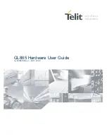
shows the timing values description in the case of an active matrix display.
Figure 7-125. Timing Values Description (Active Matrix Display)
The following bit fields define the timing generation of ac-bias (output enable in active matrix mode):
•
Invert output enable (DSS.
[15] IEO bit)
•
ac-bias pin frequency (DSS.
[7:0] ACB bit field)
•
ac-bias pin transitions per interrupt (DSS.
[11:8] ACBI bit field)
•
ac-bias gated (DSS.
[8] ACBIASGATED)
The following bit fields define the timing generation of the pixel clock:
•
Pixel clock divisor (DSS.
[7:0] PCD bit field)
•
Invert pixel clock (DSS.
[14] IPC bit)
•
Pixel clock gated (DSS.
[5] PIXELCLOCKGATED bit)
The 8-bit pixel clock divider (the DSS.
[7:0] PCD bit field) selects the pixel clock
frequency. This bit field generates a range of pixel clock frequencies from LC/1 to LC/255, where LC is the
logic clock from the divided functional clock of the display controller by the DSS.
LCD bit field.
The pixel clock is defined by the following equation:
1730
Display Subsystem
SWPU177N – December 2009 – Revised November 2010
Copyright © 2009–2010, Texas Instruments Incorporated
Содержание OMAP36 Series
Страница 174: ...174 List of Tables SWPU177N December 2009 Revised November 2010 Copyright 2009 2010 Texas Instruments Incorporated ...
Страница 692: ...692 MPU Subsystem SWPU177N December 2009 Revised November 2010 Copyright 2009 2010 Texas Instruments Incorporated ...
Страница 1084: ...1084 IVA2 2 Subsystem SWPU177N December 2009 Revised November 2010 Copyright 2009 2010 Texas Instruments Incorporated ...
Страница 1990: ...1990 2D 3D Graphics Accelerator SWPU177N December 2009 Revised November 2010 Copyright 2009 2010 Texas Instruments Incorporated ...
Страница 2334: ...2334 Memory Subsystem SWPU177N December 2009 Revised November 2010 Copyright 2009 2010 Texas Instruments Incorporated ...
Страница 2700: ...2700 Memory Management Units SWPU177N December 2009 Revised November 2010 Copyright 2009 2010 Texas Instruments Incorporated ...
Страница 2868: ...2868 HDQ 1 Wire SWPU177N December 2009 Revised November 2010 Copyright 2009 2010 Texas Instruments Incorporated ...
Страница 2974: ...2974 UART IrDA CIR SWPU177N December 2009 Revised November 2010 Copyright 2009 2010 Texas Instruments Incorporated ...
Страница 3054: ...3054 Multichannel SPI SWPU177N December 2009 Revised November 2010 Copyright 2009 2010 Texas Instruments Incorporated ...
Страница 3462: ...3462 MMC SD SDIO Card Interface SWPU177N December 2009 Revised November 2010 Copyright 2009 2010 Texas Instruments Incorporated ...
Страница 3508: ...3508 General Purpose Interface SWPU177N December 2009 Revised November 2010 Copyright 2009 2010 Texas Instruments Incorporated ...
Страница 3584: ...3584 Initialization SWPU177N December 2009 Revised November 2010 Copyright 2009 2010 Texas Instruments Incorporated ...
Страница 3648: ...3648 Debug and Emulation SWPU177N December 2009 Revised November 2010 Copyright 2009 2010 Texas Instruments Incorporated ...