background image

5 Nomenclature, Package Symbolization, and Revision Identification

The revision of the device can be identified by the revision letter on the 

Package Markings

 or by the 

HW_ID 

located inside the TLV structure of the device.

5.1 Device Nomenclature

To designate the stages in the product development cycle, TI assigns prefixes to the part numbers of all MSP 
MCU devices. Each MSP MCU commercial family member has one of two prefixes: MSP or XMS. These 
prefixes represent evolutionary stages of product development from engineering prototypes (XMS) through fully 
qualified production devices (MSP).

XMS

 – Experimental device that is not necessarily representative of the final device's electrical specifications

MSP

 – Fully qualified production device

Support tool naming prefixes:

X

: Development-support product that has not yet completed Texas Instruments internal qualification testing.

null

: Fully-qualified development-support product.

XMS devices and X development-support tools are shipped against the following disclaimer:

"Developmental product is intended for internal evaluation purposes."

MSP devices have been characterized fully, and the quality and reliability of the device have been demonstrated 
fully. TI's standard warranty applies.

Predictions show that prototype devices (XMS) have a greater failure rate than the standard production devices. 
TI recommends that these devices not be used in any production system because their expected end-use failure 
rate still is undefined. Only qualified production devices are to be used.

TI device nomenclature also includes a suffix with the device family name. This suffix indicates the temperature 
range, package type, and distribution format.

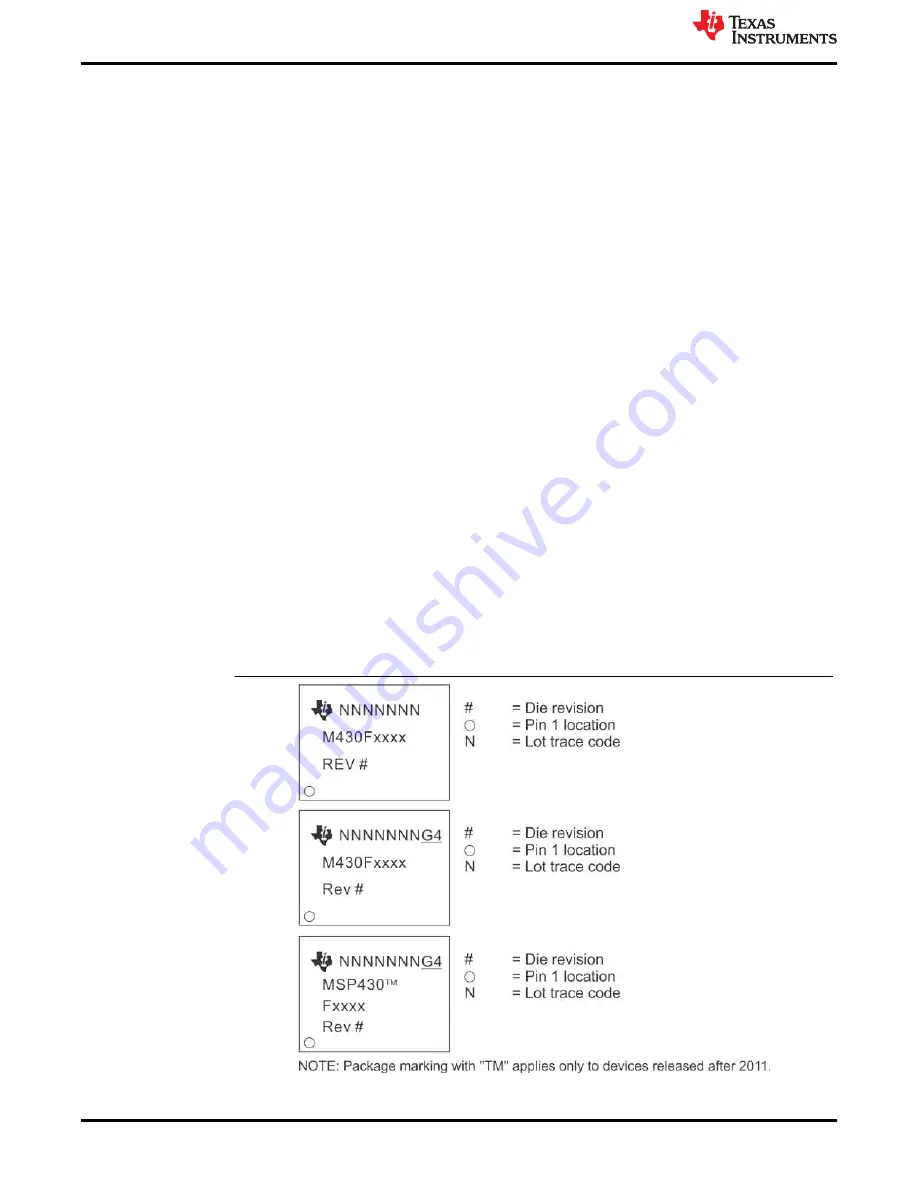
5.2 Package Markings

PZ100

LQFP (PZ) 100 Pin

Nomenclature, Package Symbolization, and Revision Identification

www.ti.com

4

MSP430F6720A Microcontroller

SLAZ657S – FEBRUARY 2015 – REVISED MAY 2021

Submit Document Feedback

Copyright © 2021 Texas Instruments Incorporated

Содержание MSP430F6720A

Страница 1: ...visories 3 4 Fixed by Compiler Advisories 3 5 Nomenclature Package Symbolization and Revision Identification 4 5 1 Device Nomenclature 4 5 2 Package Markings 4 5 3 Memory Mapped Hardware Revision TLV...

Страница 2: ...M11 PMM12 PMM14 PMM15 PMM18 PMM20 PMM26 PORT15 PORT19 SD3 UCS11 USCI36 USCI37 USCI41 USCI42 USCI47 USCI50 2 Preprogrammed Software Advisories Advisories that affect factory programmed software The che...

Страница 3: ...umber Rev B CPU21 CPU22 CPU40 Refer to the following MSP430 compiler documentation for more details about the CPU bugs workarounds TI MSP430 Compiler Tools Code Composer Studio IDE MSP430 Optimizing C...

Страница 4: ...ting null Fully qualified development support product XMS devices and X development support tools are shipped against the following disclaimer Developmental product is intended for internal evaluation...

Страница 5: ...guidance on how to locate the TLV structure and read out the HW_ID can be found in the device User s Guide www ti com Nomenclature Package Symbolization and Revision Identification SLAZ657S FEBRUARY 2...

Страница 6: ...l repeat sequence of channels ADC12CTL1 ADC12CONSEQx In addition the timer overflow flag cannot be used to detect an overflow ADC12IFGR2 ADC12TOVIFG Workaround 1 For manual trigger mode ADC12CTL0 ADC1...

Страница 7: ...vel lower levels increase probability defining the switching level in software controlled mode applicable to DVCC only Scenario 2 When a battery is connected to DVCC AUXVCC1 or AUXVCC2 as the first vo...

Страница 8: ...SL_REQ_JTAG_OPEN in the return value has been disabled in this device Workaround None CPU21 CPU Module Category Compiler Fixed Function Using POPM instruction on Status register may result in device h...

Страница 9: ...ates an INFOD Flash memory erase the program counter is corrupted Workaround None NOTE This erratum applies to debug mode only CPU40 CPU Module Category Compiler Fixed Function PC is corrupted when ex...

Страница 10: ...st Stack Pointer increment is followed by an unintended read access to the memory If this read access is performed on vacant memory the VMAIFG will be set and can trigger the corresponding interrupt S...

Страница 11: ...on e g ret push call pop jmp br is fetched from the last addresses last 4 or 8 byte of a memory e g FLASH RAM FRAM that is not contiguous to a higher valid section on the memory map In debug mode usin...

Страница 12: ...nfigured to transfer bytes from the eUSCI_A or eUSCI_B transmit or receive buffers the transmit or receive triggers TXIFG and RXIFG may not be seen by the DMA module and the transfer of the bytes is m...

Страница 13: ...d the line that clears the DMAEN bit the DMA always requests the bus and the JTAG system never gains control of the device Workaround When operating the DMA in repeat burst block transfer mode set bre...

Страница 14: ...eliable debug session or general issues with JTAG device connectivity and the resulting bad customer experience Texas Instruments has chosen to remove the LPMx 5 debug support feature from common MSP4...

Страница 15: ...n Programmer use v1 2 3 0 or later 3 For custom programming solutions refer to the specification on MSP430 Programming Via the JTAG Interface User s Guide SLAU320 revision V or newer and use MSPDebugS...

Страница 16: ...rmance mode and mask CPU execution for 150 us on wakeup from LPM3 and LPM4 However when the low side SVS and the SVM are disabled or are operating in full performance mode SVMLE 0 and SVSLE 0 or SVMLF...

Страница 17: ...ode SVSMLCTL SVSLFP 0 This provides a settling time delay of approximately 150us allowing the core sufficient time to increase to the expected voltage before the delay expires PMM15 PMM Module Categor...

Страница 18: ...e wakeup time from LPM2 3 4 to twakeupslow 150 us or Do not configure the SVSH SVMH such that the modules transition from Normal mode to an OFF state on LPM entry and ensure SVSH SVMH is in manual mod...

Страница 19: ...In this mode a POR should typically be triggered when DVCC reaches 3 75V If the OVP feature of SVM high side is enabled going into LPM234 the SVM might trigger at DVCC voltages below 3 6V 3 5V within...

Страница 20: ...o SVSMLCTL and only if the code that checks for SVSMLDLYIFG 1 is implemented without a timeout The device will be stuck in the polling loop polling since SVSMLDLYIFG will never be cleared Workaround F...

Страница 21: ...CSCTL4 register will correctly configure the respective clock to use the intended clock source but might also erroneously set XT1 XT2 fault flag if the crystals are not present at XT1 XT2 or not confi...

Страница 22: ...stuck to 1 or start toggling after transmission is completed This happens in all four combinations of Clock Phase and Clock Polarity options UCAxCTLW0 UCCKPH UCAxCTLW0 UCCKPL bits as well as in Master...

Страница 23: ...to detect communication failure condition where UCRXIFG is not set check both UCRXIFG and UCTXIFG If UCTXIFG is set twice but UCRXIFG is not set reset the MSP SPI slave by setting and then clearing th...

Страница 24: ...2019 to May 11 2021 Page Changed the document format and structure updated the numbering format for tables figures and cross references throughout the document 6 Revision History www ti com 24 MSP430...

Страница 25: ...are subject to change without notice TI grants you permission to use these resources only for development of an application that uses the TI products described in the resource Other reproduction and...

Отзывы: