background image

www.ti.com

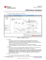
Doubler: Can double input signal frequency (input must be 50% duty cycle to use this)

Pre-R divider: Divides frequencies up to 1400 MHz

Multiplier: Multiplies frequencies between 40 to 70 MHz and outputs between 180 to 250 MHz

R divider: Used for dividing frequencies below 5 MHz for very low PFD

Charge Pump Gain: This tab will auto-update both UP and DN to be equal. Go to bits/pins section
if you want to force different values.

Gain multiplier: Multiplies Charge Pump Gain by a factor

State: Changes the charge pump output state

FCAL_EN: Every time you change the output frequency, toggle this off or on to calibrate the device
to the frequency.

Fvco: Set the VCO frequency between 3550 to 7100 MHz.

Divider MUX: This determines which of the 3 segments is included for a total division between 2 to
192.

Output MUX: Selects the signal from the VCO output or the Divider.

Power Settings: Changes the output power (increase 0 to 31, then additional boost with 49 to 63).

5. Burst Mode

Enter a register in

Load Register

or delay in seconds.

You can run and stop the commands in a single burst or continuous loop.

7

SNAU194 – December 2015

EVM Software Navigation

Submit Documentation Feedback

Copyright © 2015, Texas Instruments Incorporated

Содержание LMX2582EVM

Страница 1: ...LMX2582EVM High Performance Wideband PLLatinum RF Synthesizer Evaluation Board Operating Instructions User s Guide Literature Number SNAU194 December 2015 ...

Страница 2: ... Board Setup 3 2 EVM Software Startup Instructions 5 3 EVM Software Navigation 6 4 Schematic 8 5 BOM 9 6 Layout 11 2 Contents SNAU194 December 2015 Submit Documentation Feedback Copyright 2015 Texas Instruments Incorporated ...
Страница 3: ...input b Option 2 MUST switch R14p to R14 which routes the input signal from the OSCinP SMA connector instead of on board Oscillator Set a low phase noise signal generator to 100 MHz with 6 dBm power level Connect to OSCinP or OSCinM if you have a single ended signal Connect to both if you have a differential signal NOTE Phase noise of input signal should be below 150 dBc Hz at 10 kHz offset for 10...

Страница 4: ...nused output if you are using only single end Use a balan if you are using differential ended 4 Programming Interface a Connect your laptop to the EVM as shown with included USB2ANY module 4 Evaluation Board Setup SNAU194 December 2015 Submit Documentation Feedback Copyright 2015 Texas Instruments Incorporated ...
Страница 5: ... Download TICS software from TI com http www ti com tool TICSPRO SW 2 To start the EVM software open TICS exe from installed directory 5 SNAU194 December 2015 EVM Software Startup Instructions Submit Documentation Feedback Copyright 2015 Texas Instruments Incorporated ...

Страница 6: ...top menu Click PLL VCO and select LMX2582 3 Left Panel User Controls Here you can configure registers organized by function Hover your mouse over the register and its information will appear in the Context tab on the left panel Raw Registers See the entire register map Enter a HEX value in to the Data cell then click Write Register to program that value To read registers you must have MUXout pin p...

Страница 7: ...arge pump output state FCAL_EN Every time you change the output frequency toggle this off or on to calibrate the device to the frequency Fvco Set the VCO frequency between 3550 to 7100 MHz Divider MUX This determines which of the 3 segments is included for a total division between 2 to 192 Output MUX Selects the signal from the VCO output or the Divider Power Settings Changes the output power incr...

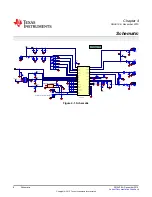
Страница 8: ...0 R36 0 1µF C11 0 R21 0 1µF C12 0 R23 0 1µF C20 0 R35 0 R37 0 1µF C25 0 R39 MUXout 10µF C21 10 µF C23 10 µF C22 10 µF C27 10 µF C24 1 µF C26 1µF C10 0 1µF C8 0 1µ F C9 External Input Frequency Option Pin5_TP Pin28_TP Pin32_TP 1 2 3 4 5 RFoutAP 142 0701 851 49 9 R33 100pF C18 VccRF 0 1µF C30 10µF C29 10µF C2 0 R1 0 1µF C1 0 1µF C16 VccRF 0 R30 0 R38 0 1µF C28 CE 1 GND 2 VBIASVCO 3 GND 4 NC 5 GND 6 ...

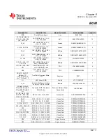
Страница 9: ...C190GKT 1 Inductor Multilayer Air Core L1 L2 MuRata LQG15HS18NJ02D 2 18 nH 0 3 A 0 36 Ω SMD OSCinM OSCinP RFoutAM RFoutAP Connector SMT End launch Emerson Network Power 142 0701 851 7 RFoutBM RFoutBP SMA 50 ohm Connectivity VCC R1 R2 R4_LF R10 R13 R21 R22 R23 RES 0 Ω 5 0 1W 0603 Vishay Dale CRCW06030000Z0EA 12 R30 R35 R37 R38 R2_LF RES 150 5 0 1 W 0603 Vishay Dale CRCW0603150RJNEA 1 R3_LF RES 12 5...

Страница 10: ...inum RF Synthesizer Texas Instruments LMX2582RHAR 1 RHA0040C Header shrouded 100mil uWire FCI 52601 S10 8LF 1 5x2 Gold plated SMD OSC 100 0000 MHZ 3 3 V 25 Y1 Connor Winfield CWX813 100 0M 1 PPM SMD 10 BOM SNAU194 December 2015 Submit Documentation Feedback Copyright 2015 Texas Instruments Incorporated ...
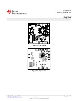
Страница 11: ...Chapter 6 SNAU194 December 2015 Layout Figure 6 1 Top Overlay Figure 6 2 Top Solder 11 SNAU194 December 2015 Layout Submit Documentation Feedback Copyright 2015 Texas Instruments Incorporated ...
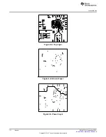
Страница 12: ...www ti com Figure 6 3 Top Layer Figure 6 4 Ground Layer Figure 6 5 Power Layer 12 Layout SNAU194 December 2015 Submit Documentation Feedback Copyright 2015 Texas Instruments Incorporated ...
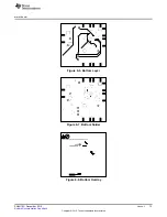
Страница 13: ...www ti com Figure 6 6 Bottom Layer Figure 6 7 Bottom Solder Figure 6 8 Bottom Overlay 13 SNAU194 December 2015 Layout Submit Documentation Feedback Copyright 2015 Texas Instruments Incorporated ...

Страница 14: ...www ti com Figure 6 9 Drill Drawing Figure 6 10 Board Dimensions 14 Layout SNAU194 December 2015 Submit Documentation Feedback Copyright 2015 Texas Instruments Incorporated ...

Страница 15: ...ring the warranty period to the address designated by TI and that are determined by TI not to conform to such warranty If TI elects to repair or replace such EVM TI shall have a reasonable time to repair such EVM or provide replacements Repaired EVMs shall be warranted for the remainder of the original warranty period Replaced EVMs shall be warranted for a new full ninety 90 day warranty period 3 ...

Страница 16: ... by Industry Canada to operate with the antenna types listed in the user guide with the maximum permissible gain and required antenna impedance for each antenna type indicated Antenna types not included in this list having a gain greater than the maximum gain indicated for that type are strictly prohibited for use with this device Concernant les EVMs avec antennes détachables Conformément à la rég...

Страница 17: ... connecting any load to the EVM output If there is uncertainty as to the load specification please contact a TI field representative During normal operation even with the inputs and outputs kept within the specified allowable ranges some circuit components may have elevated case temperatures These components include but are not limited to linear regulators switching transistors pass transistors cu...

Страница 18: ...F REMOVAL OR REINSTALLATION ANCILLARY COSTS TO THE PROCUREMENT OF SUBSTITUTE GOODS OR SERVICES RETESTING OUTSIDE COMPUTER TIME LABOR COSTS LOSS OF GOODWILL LOSS OF PROFITS LOSS OF SAVINGS LOSS OF USE LOSS OF DATA OR BUSINESS INTERRUPTION NO CLAIM SUIT OR ACTION SHALL BE BROUGHT AGAINST TI MORE THAN ONE YEAR AFTER THE RELATED CAUSE OF ACTION HAS OCCURRED 8 2 Specific Limitations IN NO EVENT SHALL T...

Страница 19: ...esponsible for compliance with all legal regulatory and safety related requirements concerning its products and any use of TI components in its applications notwithstanding any applications related information or support that may be provided by TI Buyer represents and agrees that it has all the necessary expertise to create and implement safeguards which anticipate dangerous consequences of failur...

Отзывы: