background image

MODE SELECTION 

JUMPER

ENABLE OFF 

JUMPER

PGOOD SELECTION 

JUMPER

Setup

www.ti.com

4

SNVU670A – February 2020 – Revised June 2020

Submit Documentation Feedback

Copyright © 2020, Texas Instruments Incorporated

LMR36506MSCEVM User’s Guide

1.2

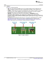
Jumpers

See

Figure 3

for jumper locations.

JEN -

This jumper allows the ENABLE input to be connected to GND in order to disable the IC. By

default, this jumper is left open since there is a pullup resistor R2 (RENT) to VIN to enable the IC.

JPGOOD -

Use this jumper to select how the PGOOD pin can be connected. A jumper can be used to

connect pin 2 and 3. In this configuration, the PGOOD pin will be pulled up to VOUT through R9
(RPGOOD) with a value of 100 k

Ω

. By default, this jumper is left open.

JMODE/RT -

Use this jumper to select the mode of operation in a

MODE/SYNC

trim part.

Connecting a jumper between pin 1 and 2 cause the IC to operate in PFM (Pulse Frequency
Modulation) mode for a higher efficiency at light load. A jumper between pin 2 and pin 3 causes the IC
to operate in FPWM mode (Forced Pulse Width Modulation) mode. By default, the jumper is connected
between pin 1 and 2.
In an

RT

trim part, connecting this jumper from pin 1 and 2 sets the switching frequency to 2.2 MHz

and connecting this jumper from pin 2 and 3 sets the switching frequency to 1 MHz. See the

LMR36506-Q1 3-V–65-V, 0.6-A Synchronous Buck Converter Optimized for Size and Light Load
Efficiency

data sheet for more information on switching frequency configuration.

Figure 3. Jumper Locations

Содержание LMR36506MSCEVM

Страница 1: ... an easy to use synchronous step down DC DC converter capable of driving up to 0 6 A of load current from an input voltage of up to 65 V The LMR36506MSCEVM features an output voltage of 5 V and a switching frequency of 2 2 MHz See the LMR36506 Q1 3 V 65 V 0 6 A Synchronous Buck Converter Optimized for Size and Light Load Efficiency data sheet for additional features detailed descriptions and avail...

Страница 2: ...VOUT Efficiency 11 11 LMR36506MSCEVM 5 VOUT Load Regulation 11 12 LMR36506MSCEVM Load Transient 12 VIN 5 VOUT IOUT 0 3 A to 0 6 A TR TF 1 µs CH1 VOUT CH4 IOUT 11 13 LMR36506MSCEVM Output Ripple 12 VIN 5 VOUT IOUT 0 A 11 14 LMR36506MSCEVM 5 VOUT Thermal Capture 12 VIN 0 6 A Load 2 2 MHz 12 15 LMR36506MSCEVM 5 VOUT Thermal Capture 24 VIN 0 6 A Load 2 2 MHz 12 16 LMR36506MSCEVM CISPR25 Conducted EMI ...

Страница 3: ...D_EMI Ground connection for the input supply VIN Input supply to the IC Can be connected to DMM to measure input voltage after EMI filter VOUT Output voltage test point of EVM Can be connected to a desired load GND Ground test points EN This test point is connected to the EN pin By default there is a pullup resistor R2 RENT to VIN to enable the IC PGOOD This test point is connected to the PGOOD pi...

Страница 4: ...rough R9 RPGOOD with a value of 100 kΩ By default this jumper is left open JMODE RT Use this jumper to select the mode of operation in a MODE SYNC trim part Connecting a jumper between pin 1 and 2 cause the IC to operate in PFM Pulse Frequency Modulation mode for a higher efficiency at light load A jumper between pin 2 and pin 3 causes the IC to operate in FPWM mode Forced Pulse Width Modulation m...

Страница 5: ...ly between the VIN_EMI and GND_EMI test points 2 Connect the load between the VOUT and GND test points 3 Set the supply voltage at an appropriate level between 5 5 V to 65 V Set the current limit of the supply to an appropriate level 4 Turn on the power supply With the default configuration the EVM powers up and provides VOUT 5 V 5 Monitor the output voltage The maximum load current must be 0 6 A ...

Страница 6: ... R2 RENT TP10 SYNC TP11 EN TP9 PGOOD TP2 GND VIN 5 5V 65V 2 2uF C1 CIN1 2 2uF C9 CIN3 0 1uF C11 Cfilt1 0 1uF C12 Cfilt2 VINF 100k R3 RFBT 24 9k R7 RFBB MODE SYNC 1 PGOOD 2 EN UVLO 3 VIN 4 SW 5 BOOT 6 VCC 7 FB 8 GND 9 LMR36506MSCQRPETQ1 U1 GND 22uF C5 COUT1 22uF C10 COUT2 DNP 10pF C13 CFF DNP 0 R4 RMODE VOUT 5V B A 6 8µH L1 1nF C14 COUTHF Schematic www ti com 6 SNVU670A February 2020 Revised June 2...

Страница 7: ...yout 7 SNVU670A February 2020 Revised June 2020 Submit Documentation Feedback Copyright 2020 Texas Instruments Incorporated LMR36506MSCEVM User s Guide 4 Board Layout Figure 5 Top View of EVM Figure 6 EVM Top Copper Layer ...

Страница 8: ...t www ti com 8 SNVU670A February 2020 Revised June 2020 Submit Documentation Feedback Copyright 2020 Texas Instruments Incorporated LMR36506MSCEVM User s Guide Figure 7 EVM Mid Layer One Figure 8 EVM Mid Layer Two ...

Страница 9: ...ww ti com Board Layout 9 SNVU670A February 2020 Revised June 2020 Submit Documentation Feedback Copyright 2020 Texas Instruments Incorporated LMR36506MSCEVM User s Guide Figure 9 EVM Bottom Copper Layer ...

Страница 10: ...iducial Fiducial mark There is nothing to buy or mount N A N A 0 J1 J2 JPGOOD JMODE RT Header 100mil 3x1 Gold TH Samtec HTSW 103 07 G S 2 J3 JEN Header 100mil 2x1 Gold TH Samtec HTSW 102 07 G S 1 L1 74438336068 FIXED IND 6 8UH 1 6A 193 MOHM Wurth Electronics 74438336068 1 L3 FBMH3225HM601N T Ferrite Bead 600 ohm 100 MHz 3 A 1210 Taiyo Yuden FBMH3225HM601NT 1 R1 RENB RES 100 k 1 0 063 W AEC Q200 Gr...

Страница 11: ...nts Incorporated LMR36506MSCEVM User s Guide 6 Test Results Section 6 1 details the test results from the LMR36506MSCEVM variant 6 1 LMR36506MSCEVM Test Results The LMR36506MSCEVM variant is used for all figures from Figure 10 to Figure 17 variant 6 1 1 Efficiency and Load Regulation Figure 10 LMR36506MSCEVM 5 VOUT Efficiency Figure 11 LMR36506MSCEVM 5 VOUT Load Regulation 6 1 2 Load Transients Fi...

Страница 12: ...re Figure 14 LMR36506MSCEVM 5 VOUT Thermal Capture 12 VIN 0 6 A Load 2 2 MHz Figure 15 LMR36506MSCEVM 5 VOUT Thermal Capture 24 VIN 0 6 A Load 2 2 MHz 6 1 4 Conducted EMI Figure 16 LMR36506MSCEVM CISPR25 Conducted EMI Results 13 5 VIN 5 VOUT IOUT 0 6 A Blue Average and Yellow Peak Figure 17 LMR36506MSCEVM CISPR25 Conducted EMI Results 13 5 VIN 5 VOUT IOUT 0 6 A Blue Average and Yellow Peak ...

Страница 13: ...s for previous revisions may differ from page numbers in the current version Changes from Original February 2020 to A Revision Page Updated EVM board image 1 Updated EVM board connections image 3 Updated LMR36506MSCEVM schematic 6 Updated top PCB view image 7 Updated top copper layer image 7 Updated EVM mid layer one image 8 Updated EVM mid layer two image 8 Updated EVM bottom copper layer image 9...

Страница 14: ...other than TI b the nonconformity resulted from User s design specifications or instructions for such EVMs or improper system design or c User has not paid on time Testing and other quality control techniques are used to the extent TI deems necessary TI does not test all parameters of each EVM User s claims against TI under this Section 2 are void if User fails to notify TI of any apparent defects...

Страница 15: ... These limits are designed to provide reasonable protection against harmful interference in a residential installation This equipment generates uses and can radiate radio frequency energy and if not installed and used in accordance with the instructions may cause harmful interference to radio communications However there is no guarantee that interference will not occur in a particular installation...

Страница 16: ...y for convenience and should be verified by User 1 Use EVMs in a shielded room or any other test facility as defined in the notification 173 issued by Ministry of Internal Affairs and Communications on March 28 2006 based on Sub section 1 1 of Article 6 of the Ministry s Rule for Enforcement of Radio Law of Japan 2 Use EVMs only after User obtains the license of Test Radio Station as provided in R...

Страница 17: ... any interfaces electronic and or mechanical between the EVM and any human body are designed with suitable isolation and means to safely limit accessible leakage currents to minimize the risk of electrical shock hazard User assumes all responsibility and liability for any improper or unsafe handling or use of the EVM by User or its employees affiliates contractors or designees 4 4 User assumes all...

Страница 18: ...OR DAMAGES ARE CLAIMED THE EXISTENCE OF MORE THAN ONE CLAIM SHALL NOT ENLARGE OR EXTEND THIS LIMIT 9 Return Policy Except as otherwise provided TI does not offer any refunds returns or exchanges Furthermore no return of EVM s will be accepted if the package has been opened and no return of the EVM s will be accepted if they are damaged or otherwise not in a resalable condition If User feels it has...

Страница 19: ...se resources are subject to change without notice TI grants you permission to use these resources only for development of an application that uses the TI products described in the resource Other reproduction and display of these resources is prohibited No license is granted to any other TI intellectual property right or to any third party intellectual property right TI disclaims responsibility for...

Отзывы: