


PLL Loop Filters and Loop Parameters
6
SNAU252 – June 2020
Copyright © 2020, Texas Instruments Incorporated
LMK04832EVM-CVAL User’s Guide
of 1 and 2 works in conjunction with control on this list #14, SYSREF_GBL_PD.
26. CLKoutY_FMT: Set the clock output format for CLKoutY.
27. Clock output frequency for CLKoutX and CLKoutY.
2.1.2
TICS Pro Tips
Mousing over different controls will display a help prompt with the register address, the data bit location
and length, and a brief register description in the lower-left
Context
help pane.
Setting a register equal to 0 or un-checking a register’s checkbox performs the same action. Similarly,
setting a register equal to 1
is the same as
checking that register’s checkbox.
3
PLL Loop Filters and Loop Parameters
In jitter cleaning applications that use a cascaded or dual PLL architecture, the first PLL’s purpose is to
substitute the phase noise of a low-noise oscillator (VCXO) for the phase noise of a dirty reference clock.
The first PLL is typically configured with a narrow loop bandwidth to minimize the impact of the reference
clock phase noise. The reference clock consequently serves only as a frequency reference rather than a
phase reference.
The loop filters on the LMK04832EVM-CVAL evaluation board are setup using the approach above. The
loop filter for PLL1 has been configured for a narrow loop bandwidth (< 1 kHz). The specific loop
bandwidth values depend on the phase noise performance of the oscillator mounted on the board.
and
contain the parameters for PLL1 and PLL2 for each oscillator option.
TI’s PLLatinum™ Sim tool can be used to optimize PLL phase noise/jitter for given specifications. See
http://www.ti.com/tool/pllatinumsim-sw
for more information.
3.1
PLL1 Loop Filter
(1)
Loop Bandwidth is a function of K
φ
, Kvco, N as well as loop components. Changing K
φ
and N will change the loop bandwidth.
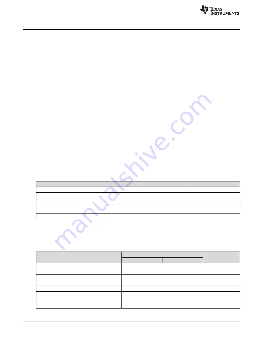
Table 2. PLL1 Loop Filter Parameters for Crystek 122.88-MHz VCXO
(1)
122.88-MHz VCXO PLL
Phase Margin
50
˚
K
φ
(Charge Pump)
450 µA
Loop Bandwidth
14 Hz
Phase Detector Freq
1.024 MHz
VCO Gain
2.5 kHz/V
Reference Clock Frequency
122.88 MHz
Output Frequency
122.88 MHz
(To PLL 2)
Loop Filter Components
LF1_C1 (C75) = 100 nF
LF1_C2 (C73) = 680 nF
LF1_R2 (R64) = 39 k
Ω
3.2
PLL2 Loop Filter
(1)
PLL Loop Bandwidth is a function of K
φ
, Kvco, N as well as loop components. Changing K
φ
and N will change the loop
bandwidth.
Table 3. Integrated VCO PLL
(1)
PARAMETER
LMK04832-SP
UNIT
VCO0
VCO1
LF2_C1 (C58)
0.047
nF
LF2_C2 (C56)
3.9
nF
C3 (internal)
0.03
nF
C4 (internal)
0.01
nF
LF2_R2 (R41)
0.62
k
Ω
R3 (internal)
0.2
k
Ω
R4 (internal)
0.2
k
Ω
Charge Pump Current, K
φ
3.2
mA


